Download
1 / 21
210 likes | 429 Views
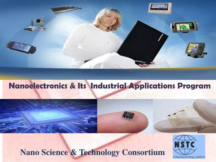
Nanoelectronics & Its Industrial Applications Program. Nano Science & Technology Consortium. What is Nanoelectronics ?. Nanoelectronics is one of the major technologies of Nanotechnology . It plays vital role in the field of engineering and electronics.

E N D
Nanoelectronics & Its Industrial Applications Program Nano Science & Technology Consortium
What is Nanoelectronics ? • Nanoelectronics is one of the major technologies of Nanotechnology. It plays vital role in the field of engineering and electronics. • Nanoelectronics make use of scientific methods at atomic scale for developing the Nano machines. The main target is to reduce the size, risk factor and surface areas of the materials and molecules. Machines under nano electronic process undergoes the long range of manufacturing steps each with accurate molecular treatment. Nano Science & Technology Consortium
What is Nanoelectronics ?-Contd. • The Nanotechnology field has been the subject of intense focus, particularly from the viewpoint of the electronics industry. The commitment is, no doubt, driven to a large measure by the current top-down methodologies for fabrication of silicon-based devices. This is implied in the next-generation approach towards manufacture of MEMS, microprocessors, optical switching and several other electronic components. • Nanotechnology is expected to bring about improvisation in deposition, implantation, lithography and metrology, thus supporting scaling up of silicon CMOS and is eventually expected to replace CMOS. Nano Science & Technology Consortium
Advantages of Nanoelectronics • One of the obvious advantage is that Nanoelectronics reduces size and scale of the machine with the help of complex integration on the circuit silicon chips. • Advanced properties of semiconductors can be determined with the help of Nanoelectronics. • Molecular scale Nanoelectronics is also known as “the next step” in the miniaturization of electronic devices, with latest electronics theory and research in the field of nanoelectronics, it is possible to explore the diverse properties of molecules. • Extreme fabrication also supported the multiple use of single machine. Parallel processing is also empowered by Nanoelectronics. Nano Science & Technology Consortium
Industrial Applications & World Market • Nanotechnology is continually playing vital role to improve the capability of electronic products. The technology also made the devices very light making the product easy to carry or move and at the same time it has reduced the power requirement. Some Consumer Products which are using Nanotechnology: • Computer Hardware • Display Devices • Mobile & Communication Products • Audio Products • Camera & Films • The world market for nanoelectronics is expected to reach $409.6 billion by 2015. Nano Science & Technology Consortium
Career Aspects Major Industries in Electronics Using Nanotechnology in their Products • Samsung® • AMD® • a123systems • Starkey, Inc. • Multiple Manufacturers • IBM® • Apple®, Inc. • Intel® • Eikos® Inc. • IOGEAR®, Inc. • Lenovo • LG® Electronics • Asahi® Glass Co., Ltd. Nano Science & Technology Consortium
Career Aspects-Contd. Various Positions in Electronics/ Electrical/ Communication Industries in the area of Nano scale fabrication, Micro/Nano electromechanical systems (in Engineering/Management domains). Some of them are given below: • Service Engineer (Microscopy) • Research Scientist (Materials – Photovoltaic’s) • Application and Business Support Engineer • Research Assistant/Associate • Solar Energy Competitive Intelligence Leader • Development Engineer (Wafer Fabrication) • Senior Wafer Fabrication Process Engineer (Etching) • Senior Wafer Fabrication Process Engineer (Photolithography) • Senior Research Engineer (Packaging Reliability) • Senior Research Engineer (Circuit designer) • Senior Research Engineer/Officer (Millimeter Wave and Modeling) • Senior Research Engineer (MEMS Sensor Design) • Market and Technology Development Manager Nano Science & Technology Consortium
Program Ingredients Program Contains Printed Study Material:To some of extent printed materials will be provided to the participants. Online Material: Some of the module contents will be provided online only. Nano Science & Technology Consortium
Program Delivery Methodology • Program Organization • Syllabus: Organized on main page in the form of course modules . • Course Updates • Glossary • Online Assignment, Quizzes, Exams & Evaluation. • Online Assistance through • Chat with faculty • e-mails • Discussion • Grade Books Nano Science & Technology Consortium
Regular Study Schedule • Participants log on to http://nstc.celnet.in for 24x7 using user-id and password to access the material. • Supplementary printed material will be provided to enhance learning in some of the modules besides online materials. Nano Science & Technology Consortium
Entering the e-Learning Zone • Participants use their user-id and password on this page to enter into the e-Learning zone. Nano Science & Technology Consortium
Accessing the Program Contents • Front Page Contains • Guidelines • Important Information • Various Activities According to the Modules Nano Science & Technology Consortium
Module Wise Learning • Each Module Contains • Course Outlines • Weekly Quizzes • Self Evaluation Assignments • Study Material • Other Learning Modes • Videos • Power Point Presentations • Related Weblinks Nano Science & Technology Consortium
Learning Through Lessons & Power Point Presentations • Participants can Learn Through • Lesson wise contents • Power Point Presentations according to the contents Nano Science & Technology Consortium
Getting Latest Updates • All Participants will be Informed About • Course Updates • Latest News • Change in Schedules • Upload of Assignments and Online Exams Nano Science & Technology Consortium
Test Yourself Through Online Quizzes & Self Evaluation Assignments Nano Science & Technology Consortium
Communicate with Faculty • Contact Our Faculty Member Through • Chat Session • e-mails • Phone calls Nano Science & Technology Consortium
Final Examination • Appear in Final Online Examination • Get Assessment report • Get Evaluation Report Nano Science & Technology Consortium
NSTC Certification Get Certificate from NSTC Nano Science & Technology Consortium
In A Nutshell Up to date information and knowledge Regular assignments, quizzes & tests, scheduled in such a way that they do not interfere with daily schedules Learning at office or at home! Secure site which only enrolled participants can access 24x7 Access Easily adaptable schedules that put no pressure on the normal course of studies/work Instant feedback of exercises, assignments & quizzes Check grades anytime & anywhere just by accessing the site Close interaction with the program coordinator on one-to-one basis guidance Nano Science & Technology Consortium
Nano Science and Technology Consortium A-105, 3rd Floor, Sector-63, Noida-201301, U.P., (India). For Queries/ Concerns Tel: +91-120- 4781215-17 Mob: +91-9818206463 Website: www.nstc.in E-mail:info@nstc.in Chat: Yahoo ID- nstcchat Nano Science & Technology Consortium