Download
1 / 82
840 likes | 1.04k Views
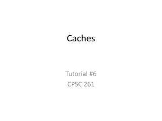
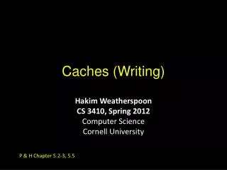
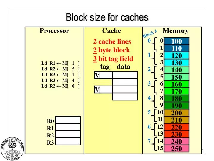
Block size for caches. Processor. Cache. Memory. Block #. 2 cache lines 2 byte block 3 bit tag field. 0 1 2 3 4 5 6 7. 0 1 2 3 4 5 6 7 8 9 10 11 12 13 14 15. 100. 110. 120. Ld R1 M[ 1 ] Ld R2 M[ 5 ] Ld R3 M[ 1 ] Ld R3 M[ 4 ]

E N D
Block size for caches Processor Cache Memory Block # 2 cache lines 2 byte block 3 bit tag field 0 1 2 3 4 5 6 7 0 1 2 3 4 5 6 7 8 9 10 11 12 13 14 15 100 110 120 Ld R1 M[ 1 ] Ld R2 M[ 5 ] Ld R3 M[ 1 ] Ld R3 M[ 4 ] Ld R2 M[ 0 ] 130 tag data 140 V 150 160 V 170 180 190 200 R0 R1 R2 R3 210 220 230 240 250
Block size for caches Processor Cache Memory 0 1 2 3 4 5 6 7 8 9 10 11 12 13 14 15 100 110 120 Ld R1 M[ 1 ] Ld R2 M[ 5 ] Ld R3 M[ 1 ] Ld R3 M[ 4 ] Ld R2 M[ 0 ] 130 tag data 140 0 150 160 0 170 180 190 200 R0 R1 R2 R3 210 220 230 240 250
Addr: 0001 Block size for caches Processor Cache Memory 0 1 2 3 4 5 6 7 8 9 10 11 12 13 14 15 100 110 120 Ld R1 M[ 1 ] Ld R2 M[ 5 ] Ld R3 M[ 1 ] Ld R3 M[ 4 ] Ld R2 M[ 0 ] 130 tag data 140 1 0 100 150 110 160 lru 0 170 180 block offset 190 200 R0 R1 R2 R3 210 110 220 Misses: 1 Hits: 0 230 240 250
Block size for caches Processor Cache Memory 0 1 2 3 4 5 6 7 8 9 10 11 12 13 14 15 100 110 120 Ld R1 M[ 1 ] Ld R2 M[ 5 ] Ld R3 M[ 1 ] Ld R3 M[ 4 ] Ld R2 M[ 0 ] 130 tag data 140 1 0 100 150 110 160 lru 0 170 180 190 200 R0 R1 R2 R3 210 110 220 Misses: 1 Hits: 0 230 240 250
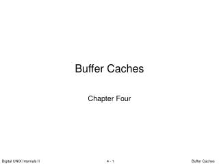
Block size for caches Processor Cache Memory 0 1 2 3 4 5 6 7 8 9 10 11 12 13 14 15 100 110 120 Ld R1 M[ 1 ] Ld R2 M[ 5 ] Ld R3 M[ 1 ] Ld R3 M[ 4 ] Ld R2 M[ 0 ] 130 tag data 140 lru 1 0 100 150 110 160 1 2 140 170 150 180 190 block offset Addr: 0101 200 R0 R1 R2 R3 210 110 220 Misses: 2 Hits: 0 150 230 240 250
Block size for caches Processor Cache Memory 0 1 2 3 4 5 6 7 8 9 10 11 12 13 14 15 100 110 120 Ld R1 M[ 1 ] Ld R2 M[ 5 ] Ld R3 M[ 1 ] Ld R3 M[ 4 ] Ld R2 M[ 0 ] 130 tag data 140 lru 1 0 100 150 110 160 1 2 140 170 150 180 190 200 R0 R1 R2 R3 210 110 220 Misses: 2 Hits: 0 150 230 240 250
Block size for caches Processor Cache Memory 0 1 2 3 4 5 6 7 8 9 10 11 12 13 14 15 100 110 120 Ld R1 M[ 1 ] Ld R2 M[ 5 ] Ld R3 M[ 1 ] Ld R3 M[ 4 ] Ld R2 M[ 0 ] 130 tag data 140 1 0 100 150 110 160 lru 1 2 140 170 150 180 190 200 R0 R1 R2 R3 210 110 220 Misses: 2 Hits: 1 150 230 110 240 250
Block size for caches Processor Cache Memory 0 1 2 3 4 5 6 7 8 9 10 11 12 13 14 15 100 110 120 Ld R1 M[ 1 ] Ld R2 M[ 5 ] Ld R3 M[ 1 ] Ld R3 M[ 4 ] Ld R2 M[ 0 ] 130 tag data 140 1 0 100 150 110 160 lru 1 2 140 170 150 180 190 200 R0 R1 R2 R3 210 110 220 Misses: 2 Hits: 1 150 230 110 240 250
Block size for caches Processor Cache Memory 0 1 2 3 4 5 6 7 8 9 10 11 12 13 14 15 100 110 120 Ld R1 M[ 1 ] Ld R2 M[ 5 ] Ld R3 M[ 1 ] Ld R3 M[ 4 ] Ld R2 M[ 0 ] 130 tag data 140 lru 1 0 100 150 110 160 1 2 140 170 150 180 190 200 R0 R1 R2 R3 210 110 220 Misses: 2 Hits: 2 150 230 140 240 250
Block size for caches Processor Cache Memory 0 1 2 3 4 5 6 7 8 9 10 11 12 13 14 15 100 110 120 Ld R1 M[ 1 ] Ld R2 M[ 5 ] Ld R3 M[ 1 ] Ld R3 M[ 4 ] Ld R2 M[ 0 ] 130 tag data 140 lru 1 0 100 150 110 160 1 2 140 170 150 180 190 200 R0 R1 R2 R3 210 110 220 Misses: 2 Hits: 2 150 230 140 240 250
Block size for caches Processor Cache Memory 0 1 2 3 4 5 6 7 8 9 10 11 12 13 14 15 100 110 120 Ld R1 M[ 1 ] Ld R2 M[ 5 ] Ld R3 M[ 1 ] Ld R3 M[ 4 ] Ld R2 M[ 0 ] 130 tag data 140 1 0 100 150 110 160 lru 1 2 140 170 150 180 190 200 R0 R1 R2 R3 210 110 220 Misses: 2 Hits: 3 140 100 230 140 240 250
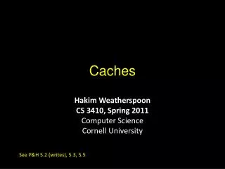
Basic Cache organization • Decide on the block size • How? Simulate lots of different block sizes and see which one gives the best performance • Most systems use a block size between 32 bytes and 128 bytes • Longer sizes reduce the overhead by: • Reducing the number of bits in each TAG • Reducing the size of each TAG Array • Very large sizes reduce the “usefulness” of the extra data • Spatial Locality – the closer it is, the more likely it will be used Address Tag Block offset
Questions to ask about a cache • What is the block size? • How many lines? • How many bytes of data storage? • How much overhead storage? • What is the hit rate? • What is the latency of an access? • What is the replacement policy ? • LRU? LFU? FIFO? Random? The Design Space is Large
What about stores? • Where should you write the result of a store? • If that memory location is in the cache? • Send it to the cache • Should we also send it to memory? (write-through policy) • If it is not in the cache? • Write it directly to memory without allocation? (write-around policy) • OR – Allocate the line (put it in the cache)? (allocate-on-write policy)
Handling stores (write-through) Processor Cache Memory 0 1 2 3 4 5 6 7 8 9 10 11 12 13 14 15 78 29 120 123 V tag data Ld R1 M[ 1 ] Ld R2 M[ 7 ] St R2 M[ 0 ] St R1 M[ 5 ] Ld R2 M[ 10 ] 71 0 150 162 0 173 18 21 33 R0 R1 R2 R3 28 19 Misses: 0 Hits: 0 200 210 225
write-through (REF 1) Processor Cache Memory 0 1 2 3 4 5 6 7 8 9 10 11 12 13 14 15 78 29 120 123 V tag data Ld R1 M[ 1 ] Ld R2 M[ 7 ] St R2 M[ 0 ] St R1 M[ 5 ] Ld R2 M[ 10 ] 71 0 150 162 0 173 18 21 33 R0 R1 R2 R3 28 19 Misses: 0 Hits: 0 200 210 225
write-through (REF 1) Processor Cache Memory 0 1 2 3 4 5 6 7 8 9 10 11 12 13 14 15 78 29 120 123 V tag data Ld R1 M[ 1 ] Ld R2 M[ 7 ] St R2 M[ 0 ] St R1 M[ 5 ] Ld R2 M[ 10 ] 71 78 1 0 150 29 162 lru 0 173 18 21 33 R0 R1 R2 R3 28 29 19 Misses: 1 Hits: 0 200 210 225
write-through (REF 2) Processor Cache Memory 0 1 2 3 4 5 6 7 8 9 10 11 12 13 14 15 78 29 120 123 V tag data Ld R1 M[ 1 ] Ld R2 M[ 7 ] St R2 M[ 0 ] St R1 M[ 5 ] Ld R2 M[ 10 ] 71 78 1 0 150 29 162 lru 0 173 18 21 33 R0 R1 R2 R3 28 29 19 Misses: 1 Hits: 0 200 210 225
write-through (REF 2) Processor Cache Memory 0 1 2 3 4 5 6 7 8 9 10 11 12 13 14 15 78 29 120 123 V tag data Ld R1 M[ 1 ] Ld R2 M[ 7 ] St R2 M[ 0 ] St R1 M[ 5 ] Ld R2 M[ 10 ] 71 lru 78 1 0 150 29 162 1 3 162 173 173 18 21 33 R0 R1 R2 R3 28 29 19 Misses: 2 Hits: 0 173 200 210 225
write-through (REF 3) Processor Cache Memory 0 1 2 3 4 5 6 7 8 9 10 11 12 13 14 15 78 29 120 123 V tag data Ld R1 M[ 1 ] Ld R2 M[ 7 ] St R2 M[ 0 ] St R1 M[ 5 ] Ld R2 M[ 10 ] 71 lru 78 1 0 150 29 162 1 3 162 173 173 18 21 33 R0 R1 R2 R3 28 29 19 Misses: 2 Hits: 0 173 200 210 225
173 173 write-through (REF 3) Processor Cache Memory 0 1 2 3 4 5 6 7 8 9 10 11 12 13 14 15 29 120 123 V tag data Ld R1 M[ 1 ] Ld R2 M[ 7 ] St R2 M[ 0 ] St R1 M[ 5 ] Ld R2 M[ 10 ] 71 1 0 150 29 162 lru 1 3 162 173 173 18 21 33 R0 R1 R2 R3 28 29 19 Misses: 2 Hits: 1 173 200 210 225
write-through (REF 4) Processor Cache Memory 0 1 2 3 4 5 6 7 8 9 10 11 12 13 14 15 173 29 120 123 V tag data Ld R1 M[ 1 ] Ld R2 M[ 7 ] St R2 M[ 0 ] St R1 M[ 5 ] Ld R2 M[ 10 ] 71 173 1 0 150 29 162 lru 1 3 162 173 173 18 21 33 R0 R1 R2 R3 28 29 19 Misses: 2 Hits: 1 173 200 210 225
29 29 write-through (REF 4) Processor Cache Memory 0 1 2 3 4 5 6 7 8 9 10 11 12 13 14 15 173 29 120 123 V tag data Ld R1 M[ 1 ] Ld R2 M[ 7 ] St R2 M[ 0 ] St R1 M[ 5 ] Ld R2 M[ 10 ] 71 lru 173 1 0 150 29 162 1 2 71 173 150 18 21 33 R0 R1 R2 R3 28 29 19 Misses: 3 Hits: 1 173 200 210 225
write-through (REF 6) Processor Cache Memory 0 1 2 3 4 5 6 7 8 9 10 11 12 13 14 15 173 29 120 123 V tag data Ld R1 M[ 1 ] Ld R2 M[ 7 ] St R2 M[ 0 ] St R1 M[ 5 ] Ld R2 M[ 10 ] 71 lru 173 1 0 29 29 162 1 2 71 173 29 18 21 33 R0 R1 R2 R3 28 29 19 Misses: 3 Hits: 1 173 200 210 225
write-through (REF 6) Processor Cache Memory 0 1 2 3 4 5 6 7 8 9 10 11 12 13 14 15 173 29 120 123 V tag data Ld R1 M[ 1 ] Ld R2 M[ 7 ] St R2 M[ 0 ] St R1 M[ 5 ] Ld R2 M[ 10 ] 71 1 5 33 29 28 162 lru 1 2 71 173 29 18 21 33 R0 R1 R2 R3 28 29 19 Misses: 4 Hits: 1 33 200 210 225
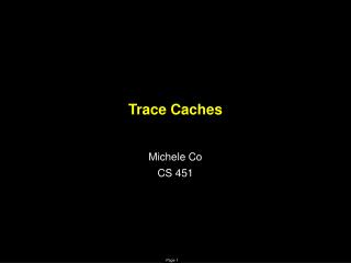
How many memory references? • Every time we STORE, we go all the way to memory • Even if we hit in the cache! caches generally miss < 10%
Write-through vs. Write-back • Can we design the cache to NOT write all stores to memory immediately? • We can keep the most current copy JUST in the cache • If that data gets evicted from the cache, update memory (a write-back policy) • We don’t want to lose the data! • Do we need to write-back all evicted blocks? • No, only blocks that have been stored into • Keep a “dirty bit”, reset when the block is allocated, set when the block is stored into. If a block is “dirty” when evicted, write its data back into memory.
Handling stores (write-back) Processor Cache Memory 0 1 2 3 4 5 6 7 8 9 10 11 12 13 14 15 78 29 120 123 V d tag data Ld R1 M[ 1 ] Ld R2 M[ 7 ] St R2 M[ 0 ] St R1 M[ 5 ] Ld R2 M[ 10 ] 71 0 150 162 0 173 18 21 33 R0 R1 R2 R3 28 19 Misses: 0 Hits: 0 200 210 225
write-back (REF 1) Processor Cache Memory 0 1 2 3 4 5 6 7 8 9 10 11 12 13 14 15 78 29 120 123 V d tag data Ld R1 M[ 1 ] Ld R2 M[ 7 ] St R2 M[ 0 ] St R1 M[ 5 ] Ld R2 M[ 10 ] 71 0 150 162 0 173 18 21 33 R0 R1 R2 R3 28 19 Misses: 0 Hits: 0 200 210 225
write-back (REF 1) Processor Cache Memory 0 1 2 3 4 5 6 7 8 9 10 11 12 13 14 15 78 29 120 123 V d tag data Ld R1 M[ 1 ] Ld R2 M[ 7 ] St R2 M[ 0 ] St R1 M[ 5 ] Ld R2 M[ 10 ] 71 1 0 0 78 150 29 162 lru 0 173 18 21 33 R0 R1 R2 R3 28 29 19 Misses: 1 Hits: 0 200 210 225
write-back (REF 2) Processor Cache Memory 0 1 2 3 4 5 6 7 8 9 10 11 12 13 14 15 78 29 120 123 V d tag data Ld R1 M[ 1 ] Ld R2 M[ 7 ] St R2 M[ 0 ] St R1 M[ 5 ] Ld R2 M[ 10 ] 71 1 0 0 78 150 29 162 lru 0 173 18 21 33 R0 R1 R2 R3 28 29 19 Misses: 1 Hits: 0 200 210 225
write-back (REF 2) Processor Cache Memory 0 1 2 3 4 5 6 7 8 9 10 11 12 13 14 15 78 29 120 123 V d tag data Ld R1 M[ 1 ] Ld R2 M[ 7 ] St R2 M[ 0 ] St R1 M[ 5 ] Ld R2 M[ 10 ] 71 lru 1 0 0 78 150 29 162 1 0 3 162 173 173 18 21 33 R0 R1 R2 R3 28 29 19 Misses: 2 Hits: 0 173 200 210 225
write-back (REF 3) Processor Cache Memory 0 1 2 3 4 5 6 7 8 9 10 11 12 13 14 15 78 29 120 123 V d tag data Ld R1 M[ 1 ] Ld R2 M[ 7 ] St R2 M[ 0 ] St R1 M[ 5 ] Ld R2 M[ 10 ] 71 lru 1 0 0 78 150 29 162 1 0 3 162 173 173 18 21 33 R0 R1 R2 R3 28 29 19 Misses: 2 Hits: 0 173 200 210 225
write-back (REF 3) Processor Cache Memory 0 1 2 3 4 5 6 7 8 9 10 11 12 13 14 15 78 29 120 123 V d tag data Ld R1 M[ 1 ] Ld R2 M[ 7 ] St R2 M[ 0 ] St R1 M[ 5 ] Ld R2 M[ 10 ] 71 1 1 0 173 150 29 162 lru 1 0 3 162 173 173 18 21 33 R0 R1 R2 R3 28 29 19 Misses: 2 Hits: 1 173 200 210 225
write-back (REF 4) Processor Cache Memory 0 1 2 3 4 5 6 7 8 9 10 11 12 13 14 15 78 29 120 123 V d tag data Ld R1 M[ 1 ] Ld R2 M[ 7 ] St R2 M[ 0 ] St R1 M[ 5 ] Ld R2 M[ 10 ] 71 1 1 0 173 150 29 162 lru 1 0 3 162 173 173 18 21 33 R0 R1 R2 R3 28 29 19 Misses: 2 Hits: 1 173 200 210 225
write-back (REF 4) Processor Cache Memory 0 1 2 3 4 5 6 7 8 9 10 11 12 13 14 15 78 29 120 123 V d tag data Ld R1 M[ 1 ] Ld R2 M[ 7 ] St R2 M[ 0 ] St R1 M[ 5 ] Ld R2 M[ 10 ] 71 lru 1 1 0 173 150 29 162 1 1 3 71 173 29 18 21 33 R0 R1 R2 R3 28 29 19 Misses: 3 Hits: 1 173 200 210 225
write-back (REF 5) Processor Cache Memory 0 1 2 3 4 5 6 7 8 9 10 11 12 13 14 15 78 29 120 123 V d tag data Ld R1 M[ 1 ] Ld R2 M[ 7 ] St R2 M[ 0 ] St R1 M[ 5 ] Ld R2 M[ 10 ] 71 lru 1 1 0 173 150 29 162 1 1 3 71 173 29 18 21 33 R0 R1 R2 R3 28 29 19 Misses: 3 Hits: 1 173 200 210 225
write-back (REF 5) Processor Cache Memory 0 1 2 3 4 5 6 7 8 9 10 11 12 13 14 15 78 173 29 120 123 V d tag data Ld R1 M[ 1 ] Ld R2 M[ 7 ] St R2 M[ 0 ] St R1 M[ 5 ] Ld R2 M[ 10 ] 71 lru 1 1 0 173 150 29 162 1 1 3 71 173 29 18 21 33 R0 R1 R2 R3 28 29 19 Misses: 4 Hits: 1 173 200 210 225
write-back (REF 5) Processor Cache Memory 0 1 2 3 4 5 6 7 8 9 10 11 12 13 14 15 173 29 120 123 V d tag data Ld R1 M[ 1 ] Ld R2 M[ 7 ] St R2 M[ 0 ] St R1 M[ 5 ] Ld R2 M[ 10 ] 71 1 0 5 33 150 28 162 lru 1 1 3 71 173 29 18 21 33 R0 R1 R2 R3 28 29 19 Misses: 4 Hits: 1 33 200 210 225
Where does write-back save us? • We write the data to memory eventually anyways – how is this better than write-through? • If a value is written repeatedly, it only gets updated in the cache. It doesn’t have to store to memory every time! • Think: loop counter, running sum, etc. • Result: less total trips to memory, lower latency for stores • If your data set fits in the cache – you can essentially skip going to memory beyond the initial load-up of program values!
What about instructions? • Instructions should be cached as well. • We have two choices: • Treat instruction fetches as normal data and allocate cache blocks when fetched. 2. Create a second cache (called the instruction cache or ICache) which caches instructions only. • What are advantages of a separate ICache? • Can anything go wrong with this?
Cache Associativity Balancing speed with capacity
Associativity • We designed a fully associative cache. • Any memory location can be copied to any cache block. • We check every cache tag to determine whether the data is in the cache. • This approach is too slow for large caches • Parallel tag searches are slow and use a lot of power • OK for a few entries…but hundreds/thousands is not feasible
Direct mapped cache • We can redesign the cache to eliminate the requirement for parallel tag lookups. • Direct mapped caches partition memory into as many regions as there are cache lines • Each memory block has a single cache line in which data can be placed. • You then only need to check a single tag – the one associated with the region the reference is located in. • Think: Modulus Hash Function
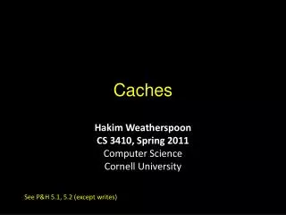
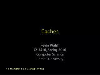
Mapping memory to cache 0 1 2 3 4 5 6 7 8 9 10 11 12 13 14 15 78 29 tag data 120 0 1 2 3 123 71 150 162 173 18 21 33 Address: 28 19 tag line index block offset 200 1 bit 2 bits 1 bit 210 225
Direct-mapped cache Processor Cache Memory 0 1 2 3 4 5 6 7 8 9 10 11 12 13 14 15 78 29 120 123 V d tag data Ld R1 M[ 1 ] Ld R2 M[ 5 ] St R2 M[ 2 ] St R1 M[ 7 ] Ld R2 M[ 4 ] 71 0 150 162 0 173 18 21 33 LRU R0 R1 R2 R3 28 19 Misses: 0 Hits: 0 200 210 225
Direct-mapped (REF 1) Processor Cache Memory 0 1 2 3 4 5 6 7 8 9 10 11 12 13 14 15 78 29 120 123 V d tag data Ld R1 M[ 1 ] Ld R2 M[ 5 ] St R2 M[ 2 ] St R1 M[ 7 ] Ld R2 M[ 4 ] 71 0 150 162 0 173 18 21 33 R0 R1 R2 R3 28 19 Misses: 0 Hits: 0 200 210 225
Direct-mapped (REF 1) Processor Cache Memory 0 1 2 3 4 5 6 7 8 9 10 11 12 13 14 15 78 29 120 123 V d tag data Ld R1 M[ 1 ] Ld R2 M[ 5 ] St R2 M[ 2 ] St R1 M[ 7 ] Ld R2 M[ 4 ] 71 1 0 0 78 150 29 162 0 173 18 21 33 R0 R1 R2 R3 28 29 19 Misses: 1 Hits: 0 200 210 225
Direct-mapped (REF 2) Processor Cache Memory 0 1 2 3 4 5 6 7 8 9 10 11 12 13 14 15 78 29 120 123 V d tag data Ld R1 M[ 1 ] Ld R2 M[ 5 ] St R2 M[ 2 ] St R1 M[ 7 ] Ld R2 M[ 4 ] 71 1 0 0 78 150 29 162 0 173 18 21 33 R0 R1 R2 R3 28 29 19 Misses: 1 Hits: 0 200 210 225
Direct-mapped (REF 2) Processor Cache Memory 0 1 2 3 4 5 6 7 8 9 10 11 12 13 14 15 78 29 120 123 V d tag data Ld R1 M[ 1 ] Ld R2 M[ 5 ] St R2 M[ 2 ] St R1 M[ 7 ] Ld R2 M[ 4 ] 71 1 0 1 71 150 150 162 0 173 18 21 33 R0 R1 R2 R3 28 29 19 Misses: 2 Hits: 0 150 200 210 225