Download
1 / 25
260 likes | 537 Views
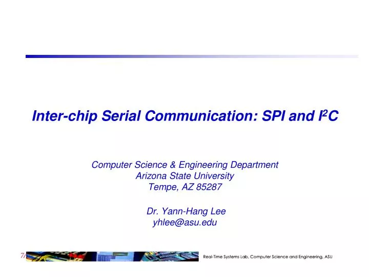
Inter-chip Serial Communication: SPI and I 2 C. Computer Science & Engineering Department Arizona State University Tempe, AZ 85287 Dr. Yann-Hang Lee yhlee@asu.edu. peripheral 1. MOSI MISO SCK SS. MOSI MISO SCK SS. MOSI MISO SCK SS1 SS2. processor. peripheral 2.

E N D
Inter-chip Serial Communication: SPI and I2C Computer Science & Engineering DepartmentArizona State University Tempe, AZ 85287 Dr. Yann-Hang Leeyhlee@asu.edu
peripheral 1 MOSI MISO SCK SS MOSI MISO SCK SS MOSI MISO SCK SS1 SS2 processor peripheral 2 Serial Peripheral Interface (SPI) • A duplex, synchronous, serial communication between CPU and peripheral devices • Master mode and slave mode • Bi-directional mode • Synchronous serial clock • Signals: • MOSI: master out slave in • MISO: master in slave out • SS: select signal from master to slave • SCK: serial clock
transmit data reg transmit data reg MOSI shift reg. shift reg. MISO receive data reg receive data reg SPI Operation • Data registers in the master and the slave form a distributed register. • When a data transfer operation is performed, this distributed register is serially shifted by the SCK clock from the master • Can shift in burst mode
CPOL and CPHA (Polarity and Phase) • CPHA=0 – the first edge on the SCK line is used to clock the first data bit (the first bit of the data must be ready when selected) • CPHA=1 – if required, the first SCK edge before the first data bit becomes available at the data out pin
Queued SPI • Queues for transmitting and receiving data, and commands. • Programmable queue to support up to 16 transfers without user intervention. • NEWQP: Start of queue pointer. This 4-bit field points to the first entry in the RAM to be executed on initiating a transfer. • ENDQP: End of queue pointer. Points to the RAM entry that contains the last transfer description in the queue. • CPTQP: Completed queue entry pointer. Points to the RAM entry that contains the last command to have been completed. • Indirect read/write – QAR[ADDR] and QDR • Wraparound enabling, chip select, etc.
Control of SPI • Mode and status • mode: master or slave. • enable • SPIF is asserted when the QSPI has completed all the commands in the queue. • transfer size, clock polarity and phase, baud rate • delays between serial transfers and clock signal • Interrupts • on SPIF • write collision in accessing RAM (by QSPI and CPU) • abort
Example 12-bit QSPI Transfer • 0xB308 QMR: set up 12-bit data words with the data shifted on the falling clock edge, and a QSPI_CLK frequency of 4.125 MHz (assuming a 66-MHz internal bus clock). • desired delays QDLYR. • 0xD00F QIR to enable write collision, abort bus errors, and clear any interrupts. • 0x0020 QAR to select the first command RAM entry. • Write QDR with commands (e.g. 0x7E00, 0x7D00, 0x7B00, 0x7700) to set up four transfers for each chip select. The chip selects are active low. • 0x0000 QAR to select the first transmit RAM entry. • Write QDR with sixteen 12-bit words of data. • 0x0F00 QWR to set up a queue beginning at entry 0 and ending at entry 15. • Set QDLYR[SPE] to enable the transfers. • Wait until the transfers are complete. QIR[SPIF] is set when the transfers are complete. • 0x0010 QAR to select the first receive RAM entry. • Read QDR to get the received data for each transfer.
I2C protocol – Background • Inter-Integrated Circuit Protocol • I2C is a low-bandwidth, short-distance, two-wire interface for communication amongst ICs and peripherals • Originally developed by Philips for TV circuits • Only two bus lines are required • The SDA(for data) and SCL(for clock) • Each device connected to the bus is software addressable • Devices can be 7-bit or 10-bit addressed
I2C Features • Simple master-slave relation amongst devices (either can be receiver or transmitter) • Multi-bus master collision detection and arbitration is supported • Serial, 8-bit oriented, bi-directional data transfer can be achieved up to100 kbit/s (and up to 3.4Mbit/s in the high speed mode) • Suppose Micro-controller A wants to send info to micro-controller B • A (master) addresses B(slave) • A (master-transmitter) sends data to B(slave-receiver) • A terminates the transfer • Suppose Micro-controller A wants to receive info from micro-controller B • A (master) addresses B(slave) • A (master-receiver) receives data from B(slave-transmitter) • A terminates the transfer
I2C Bit-Transfer • One clock pulse is generated for each data bit that is transferred • Data Validity • The data on the SDA line must be stable during the HIGH(1) period of the clock. The data line(SDA) can change data only when the clock signal (SCL) is LOW(0) • Wired-and function • open-drain or open-collector
I2C START/STOP Conditions • START condition: Signals begin of transfer (occupies the bus) • A HIGH to LOW transition on the SDA line while the SCL is HIGH • STOP condition: Signals end of transfer (releases the bus) • A LOW to HIGH transition on the SDA line while the SCL is HIGH • Both these are always generated by the Master • Repeated START condition is allowed • Repeated start is used for changing the slave, or changing the direction of data transfer (Send/Receive) for the same slave
I2C Data Transfer • Every byte on the SDA line must be 8-bits long • Each byte must be followed by an acknowledgement from the receiver • Data byte is transferred bit-wise with the MSB as the first bit sent • A slave can force the master to wait by holding the clock line SCL LOW
Acknowledgement Scheme • The acknowledge-related clock-pulse is generated by the master • The transmitter (master or slave) releases the SDA line i.e. SDA is HIGH for the ACK clock pulse • The receiver must pull-down the SDA line during the acknowledge clock pulse (stable LOW) during the HIGH period of the clock pulse
Acknowledgement Scheme • The receiver is obliged to generate an acknowledge after each byte received. • When a slave does not acknowledge slave address (when busy), it leaves the data line HIGH. The master then generates either STOP or attempts repeated START. • If a slave-receiver does ack the slave address, but some time later during the transfer can not receive more data (this is done by leaving SDA HIGH during the ack pulse), then the master either generates STOP or attempts repeated START. • If a master-receiver is involved in a transfer, it must signal the end of data to the slave-transmitter by not generating an ack on the last byte that was clocked out of the slave. The slave-transmitter must release the data line to allow the master to generate a STOP or repeated START condition.
Data Transfer With 7-Bit Device Address • After START condition (S), a slave address(7-bit) is sent. • A read/write (R/W’) direction is then sent(8th bit) • Data transfer occurs, and then always terminated by STOP condition. However, repeated START conditions can occur.
Master-Transmitter to Slave-Receiver Data Transfer • In this, the transmission direction never changes. The set-up and transfer is straight-forward
Master-Receiver and Slave-Transmitter Data Transfer • Master initiates the data transfer by generating the START condition followed by the start byte (with read/write bit set to 1 i.e. read mode) • After the first ack from the slave, the direction of data changes and the master becomes receiver and slave transmitter. • The STOP condition is still generated by the master (master sends not-ACK before generating the STOP)
Read and Write in the Same Data Transfer • Change in direction of data transfer can happen by the master generating another START condition (called the repeated START condition) with the slave address repeated • If the master was a receiver prior to the change, then the master sends a not-ack (A’) before the repeated START condition
7-Bit Addressing • The addressing info is contained in the first byte after the START condition • The first 7 bits contain the address and LSB contains the direction of transfer(R/W’ : 0 = write;1= read) • When an address is sent, each device compares the first seven bits and considers itself addressed. • A slave address can be made up of a fixed and a programmable part • PCF8575
Multi-Master Clock Synchronization • In the I2C bus, clock synchronization is performed using the wired-AND • If at least one master clock goes from HIGH to LOW, then the SCL is held LOW irrespective of the other masters’ clock. • The SCL line goes to a HIGH state only when all the master clocks are in HIGH. • The synchronized clock is generated with its LOW period determined by the device with the longest clock LOW period and its HIGH period determined by the one with the shortest clock HIGH period.
Multi-Master Arbitration Using the Clock Syn. • If more than one device is capable of being a master, then an arbitration mechanism is needed to choose the master that takes control of the bus • Arbitration takes place on the SDA, while the SCL is at the HIGH line, • the master which transmits a HIGH level, • another master is transmitting LOW level will switch off its DATA output stage because the level on the bus does not correspond to its own level.
I2C Conclusion • Compared to other serial bus protocols like SPI and Microwire • The pin (and connection) requirements are the least in I2C • The noise immunity is higher for I2C • There is a feedback to the the transmitter (Ack signal) for conveying the success of the transfer • I2C now has fast and high speed modes of operation
I2C Programming in Coldfire 5211 • Software control all I2C operations • Can be a master or slave
I2C Programming • Initialization • Set I2FDR[IC] to obtain I2C_SCL frequency from the system bus clock. • Update the I2ADR to define its slave address. • Set I2CR[IEN] to enable the I2C bus interface system. • Modify the I2CR to select or deselect master/slave mode, transmit/receive mode, and interrupt-enable or not. • As a master-transmitter • test I2SR[IBB] to determine whether the serial bus is free. • If the bus is free (IBB = 0), the START signal and the first byte (the slave address) can be sent. (I2CR[MTSA] and I2DR for slave address and R/W) • transmits next byte by write to I2DR • To stop, check I2SR[RXAK] and, if received, change I2CR[MSTA] to 0