Download
1 / 16
170 likes | 349 Views
MSP430 MSP430x1xx Texas Instruments. Presented by Akshay Saxena April 10, 2003. Features. von-Neumann architecture: All memory and peripherals are in one address space. Ultralow-power architecture: 0.1 microA – 250 microA operating current @ 1MHz. 1.8V – 3.6V operation

E N D
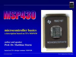
MSP430MSP430x1xxTexas Instruments Presented by Akshay Saxena April 10, 2003
Features von-Neumann architecture: All memory and peripherals are in one address space. • Ultralow-power architecture: • 0.1 microA – 250 microA operating current @ 1MHz. • 1.8V – 3.6V operation • 6 micro-sec wakeup from standby mode. • Extensive interrupt capability relieves need for polling. • Flexible and powerful processing capabilities: • Seven source-address modes. • Four destination address modes • RAM execution capability • Fast hex-to-decimal conversion • Extensive, memory-mapped peripheral set: • Integrated 12-bit A/D converter • Multiple timers • Integrated USART(s) • Watchdog Timer • Integrated programmable oscillator • Multiple I/O with extensive interrupt capability • Versatile ultra low-power device options: • Masked ROM • OTP (in-system programmable) • Flash (in-system programmable) • EPROM (UV-erasable, in-system programmable) • Up to 64K addressing space
Types of Devices • 11x • 11x1 • 11x2 • 12x • 12x2 • 13x • 14x They differ in: • Basic Clock System, Timers, I/O ports, ADC, USARTs. • Flash memory, RAM and ROM size.
Architecture • 16-bit CPU • Program memory • Data memory • Operation control • Peripheral modules • Oscillator and clock generator
CPU • RISC architecture with 27 instructions and 7 addressing modes. • Sixteen 16-bit registers (R0-R3, R4-R15). • Large 16-bit register file that reduces fetches to memory. • Single-cycle register operations. • 16-bit address and data bus. • Direct memory-to-memory transfers without intermediate register holding.
Memory • Physically separated memory areas (ROM, RAM, SFRs & peripheral modules) are mapped into common address space. • Same instructions used for code, data or peripheral accesses.
Memory • Byte instructions can use both even and odd addresses. • Word instructions can use only even addresses.
Digital I/O • Up to 6 ports (P1 – P6), each with eight I/O pins. • I/O pins are individually configured for input or output direction. • P1 and P2 with interrupt capability. • Independent input and output data registers.
Clock Module • Includes three clock sources: • LFXT1CLK – for Low / High – frequency oscillator. (low-frequency: 32kHz; high-frequency: 450kHz – 8MHz) • XT2CLK – for High-frequency oscillator. • DCOCLK – for Digitally controlled oscillator with RC-type characteristics. • Three clock signals are available: • ACLK: Auxiliary clock – for individual peripheral modules. • MCLK: Master clock – used by the CPU and system. • SMCLK: Sub-main clock – for individual peripheral modules.
Hardware Multiplier • 16-bit peripheral module. • Not integrated into the CPU; No special instructions and operates independent of CPU. • No extra cycles are required for a multiplication. • Supports four types of multiplication: • Unsigned multiplication (MPY) • Signed multiplication (MPYS) • Unsigned multiplication with accumulation (MAC) • Signed multiplication with accumulation (MACS) • Has two 16-bit registers (OP1 and OP2) for operands and three registers (ResLo, ResHi & SumExt) to store results.
Flash Memory • Internal programming voltage generation. • Bit, byte and word-addressable and programmable. • Ultralow-power operation. • Divided into segments (main and information segments) • Erase modes: single, main and all.
Applications http://www.circuitcellar.com/msp430/
References • MSP430x1xx Family – User’s Guide • http://www.ti.com/msp430