Download
1 / 1
10 likes | 137 Views
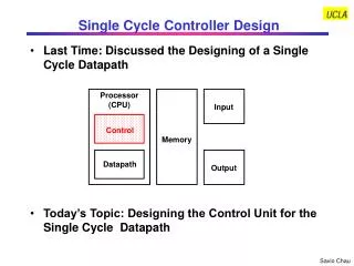
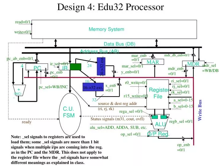
Register File. + (INC) . Design 4: Edu32 Processor. read=0/1. Memory System. write=0/1. Data Bus (DB). Address Bus (AB). mdr_db_enb=0/1. mar_enb =0/1. pc_ab_enb=0/1. MAR. ir_sel =0/1. MDR. 4. mdr_sel =WB/DB. 24. mar_sel=0/1. 24->32 ext . PC. IR. mdr_enb =0/1.

E N D
Register File + (INC) . Design 4: Edu32 Processor read=0/1 Memory System write=0/1 Data Bus (DB) Address Bus (AB) mdr_db_enb=0/1 mar_enb =0/1 pc_ab_enb=0/1 MAR ir_sel =0/1 MDR 4 mdr_sel =WB/DB 24 mar_sel=0/1 24->32 ext. PC IR mdr_enb =0/1 y_enb=0/1 pc_enb =0/1 ri_sel=0/1 16 r0_write=0/1 x_enb =0/1 rj_sel=0/1 16->32 ext. pc_sel=WB/INC rk_sel=0/1 r15_write=0/1 32 a_sel=0-15 source & dest reg addr (ri, rj, rk) b_sel=0-15 C.U. FSM Write Bus rega_sel =0/1 Status signals (m31, cout, ovfl) regb_sel =0/1 ready ALU alu_sel=ADD, ADDA, SUB, etc. op_sel =0/1 O/P Reg. Note: _sel signals to registers are used to load them; some _sel signals are more than 1 bit signals when multiple i/ps are coming into the reg. as in the PC and the MDR. This does not apply to the register file where the _sel signals have somewhat different meanings as explained in class. op_enb =0/1