Download
1 / 6
60 likes | 178 Views
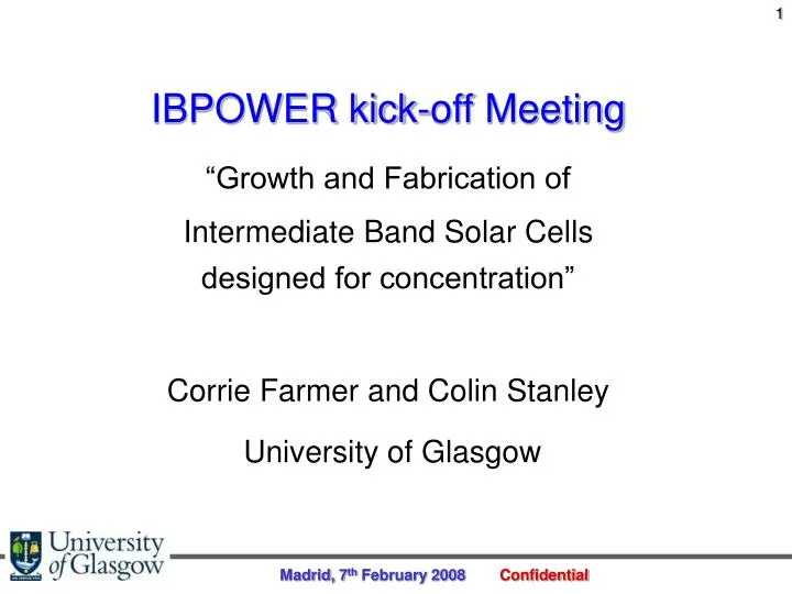
IBPOWER kick-off Meeting “Growth and Fabrication of Intermediate Band Solar Cells designed for concentration” Corrie Farmer and Colin Stanley University of Glasgow. Metal contact on p + -GaAs layer. p +. p + -GaAs. SiN x ARC, Al 0.85 Ga 0.15 As window layer.

E N D
IBPOWER kick-off Meeting “Growth and Fabrication of Intermediate Band Solar Cells designed for concentration” Corrie Farmer and Colin Stanley University of Glasgow Madrid, 7th February 2008 Confidential
Metal contact on p+-GaAs layer p+ p+-GaAs SiNx ARC,Al0.85Ga0.15As window layer IBSC - InAs QD layers incorporated into n-GaAs “base” n-GaAs n+-Al0.2Ga0.8As n+-substrate Donor impurities n-metal contact QD QD WL GaAs reference/IBSC layer structure Standard (Al,Ga)As heterojunction solar cell • QD density ~1-2x1010 cm-2 • Si d-doping to give one electron per dot • 10-50 layers of QDs Madrid, 7th February 2008 Confidential
Cross-sectional schematic Overview of device fabrication Madrid, 7th February 2008 Confidential
CB 1 IB 2 2 3 VB Solar cell characteristics (one sun) • Good efficiency of GaAs reference cell. • Lower efficiency for prototype IBSC. • Reduced VOC. • Photocurrent from IBSC due to absorption of sub-bandgap photons (2+2) with EIB-EVB<Ehf<Eg. • Photocurrent due to absorption of two sub-bandgap photons (2+3), one with Ehf~ECB-EIB Madrid, 7th February 2008 Confidential
Plans for next 6 months • Design for concentration • Minimize series resistance • Increase the open circuit voltage, Voc • MBE growth of IBSC structure • Maximize IB-CB separation (total In content per QD layer) • Maximize current produced by absorption of sub-bandgap photons (total number of QD layers) • Optimize spacer thickness between QD layers (coupled or uncoupled QDs??) • Fabrication of solar cells using; • ~5 μm thick electro-plated Au-grid for top electrode • Optimal grid geometry • Two-layer ARC • Heat sink • Characterisation by PL/EL/FTPS using FTIR spectrometer Madrid, 7th February 2008 Confidential
Further afield – strain balancing on InP In theory, this should permit an “unlimited” number of QD layers to be stacked one on top of the other V M Ustinov et al., Semiconductors Vol. 31 (10), p1080, 1997 In(Al,Ga)As layer with In fraction reduced below lattice-matched value InAs QD layer In(Al,Ga)As InP At 300 K; Eg(InP) = 1.35 eV, Eg(InAlAs) = 1.46 eV InAs QDs embedded in In0.53Ga0.47As on InP Madrid, 7th February 2008 Confidential