Download
1 / 31
310 likes | 469 Views
Steven M. Anlage Department of Physics Center for Nanophysics and Advanced Materials University of Maryland 29 October, 2008. Investigation of Microscopic Materials Limitations of Superconducting RF Cavities. SRF Materials Workshop. Questions to Address.

E N D
Steven M. Anlage Department of Physics Center for Nanophysics and Advanced Materials University of Maryland 29 October, 2008 Investigation of Microscopic Materials Limitations of Superconducting RF Cavities SRF Materials Workshop
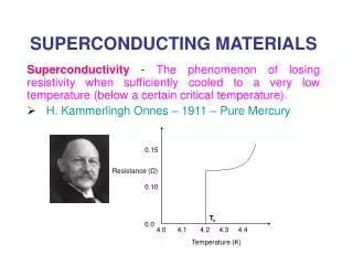
Questions to Address What new experiments shed light on limits played by topology, surface phases and structures, chemical makeup, or physics? How can we separate intrinsic behavior from that which is dependent on history or processing pathway? Are there new studies … telling us about the intrinsic qualities of the niobium surface? Do we still need to focus on heat transfer effects? My Answers: New Microscopic Techniques to link RF Properties to Local Structure Use these to establish connections between surface structure and RF performance on a microscopic scale 1) Near-Field Microwave Microscope 2) Laser Scanning Microscope
Near-Field Microwave Microscope 1 2 3 Create Strong ( BRF ~ 200 mT ) Highly Localized ( < 1 mm ) RF ( 1 - 2 GHz ) Magnetic Fields on Nb Surfaces at Low Temperatures ( < 2 K ) Microwave Microscope Probe Fundamental Response Intense BRF Drive Harmonic / Intermod Response Localized Excitation on Surface Nb Sample Measure Local Response: Nonlinearity (Harmonics, Intermodulation) Sensitive to RF breakdown, flux generation, … Correlate Local RF Properties to: Topography Defects (welds, grain boundaries, …) Surface Treatment Processing
Near-Field Microwave Microscope Example Result Third harmonic power (dBm) Localized Harmonic Generation from a single bi-crystal grain boundary in a high-Tc (YBa2Cu3O7-d) thin film << Josephson junctions are strongly nonlinear >> Harmonic Tones Out Fundamental Tone In fin = 6.5 GHz T = 60 K Phys. Rev. B 72, 024527 (2005) Superconductors have an intrinsic nonlinearity, clearly visible as J→ Jc The superfluid density is suppressed and very sensitive to perturbations rs becomes time-dependent, giving rise to harmonics and intermods
Near-Field Microwave Microscope ► Next Generation for SRF Applications ◄ Superconductors show nonlinearity due to both intrinsic and extrinsic effects Magnetic Write Heads create i) Strong RF magnetic fields: ~ 1 T in existing write heads ii) Highly localized RF magnetic fields (|| to surface!): 100’s of nm Example Result Seagate Longitudinal Recording Head 3rd-Harmonic Response of a Homogeneous high-Tc film RF Drive fin = 6.4 GHz 3rd-Harmonic Power P3f (dBm) Tc Noise Level Schematic of a longitudinal write head Temperature (K) Goals: Achieve ~200 mT surface RF fields on Nb at microwave frequencies at 2 K Image RF breakdown fields and correlate with surface properties…
1 2 3 4 Laser Scanning Microscope “Short-Sample” RF / Materials Science of Nb Surfaces Create a Microwave ( ~ GHz ) Resonance at Low Temperatures ( < 2 K ) Material of interest Microwave Input Co-planar Waveguide Resonator f0 , Q Ground Plane Perturb the Surface with a Modulated Laser Spot to cause Local Heating Measure the change in f0 and Q as the laser spot is scanned over the surface Image: JRF(x, y) Local RF Current Density Local sources of Nonlinear Response RF vortex Entry and Flow Thermal Healing Length
Laser Scanning Microscope “Short-Sample” RF / Materials Science of Nb Surfaces Reflectivity Image 1 x 8 mm scan 100 mm x 200 mm IRF RF Image BRF RF contrast developed from grain bdes, cracks, scratches, etch features, corners, etc. Low Temperature Physics 32, 592 (2006)
Laser Scanning Microscope Preliminary Results on Bulk Nb Surfaces
Determination of the Thermal Healing Length YBCO/LaAlO3 CPW Resonator T = 79 K P = - 10 dBm f = 5.285 GHz fmod = 99.9 kHz 1 x 8 mm scan Thermal Conductivity Fit gives Specific heat Mass Density Modulation Freq. Wstrip = 500 mm J. Supercond. 19, 625 (2006)
Conclusions I believe the Near-Field and Scanning Laser Microwave Microscopes can help to solve vexing SRF materials problems A proposal to DOE/HEP on SRF Materials Issues is in preparation I am looking for materials collaborators who need to solve specific materials / low-T RF property problems and think that a microscopic approach is fruitful Some topics of interest: RF properties of grain boundaries and step edges RF properties of etch pits Understanding the microscopic physics of intrinsic RF breakdown Can coatings (S / I / S /…, or novel superconductor) prolong RF breakdown? Existing Collaborators: Dragos Mircea [Seagate → Hitachi] Alexander Zhuravel [Kharkov, Ukraine] Alexey Ustinov [Karlsruhe, Germany] http://www.cnam.umd.edu/anlage/AnlageHome.htm
Directional Coupler (-6dB) f Agilent E8362 Microwave Synthesizer Cryogenicchamber Low-Pass Filters Writer High-Pass Filters sample MicrowaveAmplifiers Gain ~ 60dB f, 2f, 3f,.. Agilent E4407B Spectrum Analyzer LakeShore340Temperature Controller
New Approach: inductive writer from a HDD B ~ 1 T !!!
Pinput coaxial probe loop sample surface
The inductive reader/writer : general concept • Attractive features : • ~ T magnetic field • sub-micron pole tips
An inductive magnetic writer/reader : Example magnetic disk / superconducting sample Pins for reader/writer
An inductive magnetic writer/reader : Detail microcoils high-m magnetic core wiring of the microcoils to the pins
An inductive magnetic writer/reader : Schematics SAMPLE R. Hsiao IBM J. Res. Develop., vol. 43, no.1/2, Jan/March 1999
focused laser beam (lLAS = 670 nm, PL = 1 mW) heat source HTS film d x 21 21 21 21 21 21 substrate z 21 21 Laser-induced signal generation model The power distribution induced by a focused modulated laser beam can be described as: x-y z t spatial temporal The thermally induced changes of S21(f) in the probe are understood as LSM photo-response (PR) that can be expressed as: ~ where inductive PR + resistive PR + insertion loss PR Scanning Laser Microscopy of Superconducting Microwave Devices A.P. Zhuravel, S. M. Anlage and A.V. Ustinov
Results: Power dependence of PRR(x,y) 10 mm PRR(x,y) YBCO LAO LAO LAO YBCO +2 dBm 0 dBm 3D plot of resistive LSM PR at +6 dBm +4 dBm +6 dBm Images of resistive LSM PR penetrating into HTS film (area B) at the different input HF power indicated in the images. White dotted boxes show the YBCO/LAO patterned edge. Brighter regions correspond to larger amplitude of PRR(x,y). Scanning Laser Microscopy of Superconducting Microwave Devices A.P. Zhuravel, S. M. Anlage and A.V. Ustinov
Microwave Microscope Probe Fundamental Response Intense BRF Drive Harmonic / Intermod Response Localized Excitation on Surface Nb Sample
- 42 - 43 - 49 - 55 2f1 -f2 2f2 –f1 x y (a) (c) (b) RFOUT Y -14 -14 X 1x1 mm Power [dBm] - 42 - 43 1 mm f1 f2 Frequency RFIN 1x1 mm - YBCO film 1x1 mm - LAO substrate JRF Y X max JRF JIMD IMD PR Jrf Y Y max X X 0 0
TM010 Resonant Mode Current Distribution Fiducial Materials Nb Strip with Two different Treatment
Pb Pb defect defect Sapphire Sapphire Nb Nb
1 mm Gap Nb strip reflectivity RF = -3dBm F1
1 mm 5.6 K Line Scan LSM PR 7.2 K + peak Temperature 0 9.2 K Line scan - peak 10.6 K Pb Nb
RF input RF input Line Line Line scan scan scan Area Area Area scan scan scan Pb foil Pb foil Pb foil (50 (50 (50 m m m m) m) m) Pb foil Pb foil Pb foil (50 (50 (50 m m m m) m) m) Nb foil Nb foil m m (160 (160 m thickness) m thickness)