Download
1 / 3
30 likes | 211 Views
Nano-magnetism and high-density magnetic memory Vitali Metlushko, Department of Electrical & Computer Engineering, UIC Prime Grant Support: NSF ECS grant # ECS-0202780, Antidot and Ring Arrays for Magnetic Storage Applications and

E N D
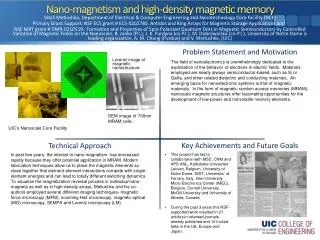
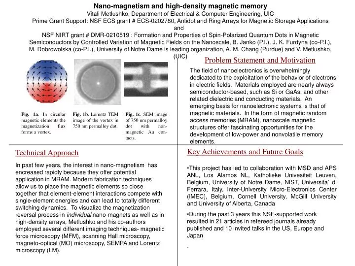
Nano-magnetism and high-density magnetic memory Vitali Metlushko, Department of Electrical & Computer Engineering, UIC Prime Grant Support: NSF ECS grant # ECS-0202780, Antidot and Ring Arrays for Magnetic Storage Applications and NSF NIRT grant # DMR-0210519 : Formation and Properties of Spin-Polarized Quantum Dots in Magnetic Semiconductors by Controlled Variation of Magnetic Fields on the Nanoscale, B. Janko (P.I.), J. K. Furdyna (co-P.I.), M. Dobrowolska (co-P.I.), University of Notre Dame is leading organization, A. M. Chang (Purdue) and V. Metlushko, (UIC) Fig. 1a. In circular magnetic elements the magnetization flux forms a vortex. Fig. 1b. Lorentz TEM image of the vortex in 750 nm permalloy dot. Fig. 1c. SEM image of 750 nm permalloy dot with non-magnetic Au con-tacts. Problem Statement and Motivation The field of nanoelectronics is overwhelmingly dedicated to the exploitation of the behavior of electrons in electric fields. Materials employed are nearly always semiconductor-based, such as Si or GaAs, and other related dielectric and conducting materials. An emerging basis for nanoelectronic systems is that of magnetic materials. In the form of magnetic random access memories (MRAM), nanoscale magnetic structures offer fascinating opportunities for the development of low-power and nonvolatile memory elements. Key Achievements and Future Goals Technical Approach In past few years, the interest in nano-magnetism has encreased rapidly because they offer potential application in MRAM. Modern fabrication techniques allow us to place the magnetic elements so close together that element-element interactions compete with single-element energies and can lead to totally different switching dynamics. To visualize the magnetization reversal process in individual nano-magnets as well as in high-density arrays, Metlushko and his co-authors employed several different imaging techniques- magnetic force microscopy (MFM), scanning Hall microscopy, magneto-optical (MO) microscopy, SEMPA and Lorentz microscopy (LM). • This project has led to collaboration with MSD and APS ANL, Los Alamos NL, Katholieke Univesiteit Leuven, Belgium, University of Notre Dame, NIST, Universita` di Ferrara, Italy, Inter-University Micro-Electronics Center (IMEC), Belgium, Cornell University, McGill University and University of Alberta, Canada • During the past 3 years this NSF-supported work resulted in 21 articles in refereed journals already published and 10 invited talks in the US, Europe and Japan • .
Nanocrystalline Carbide Derived Carbon for Tribological Applications Investigators: Michael McNallan, Civil and Materials Engineering, UIC; Ali Erdemir, Argonne National Laboratory Prime Grant Support: U.S. Department of Energy Problem Statement and Motivation max. safe temperature • Mechanical Seals and bearings fail due to frictional heating and wear • Materials used are hard ceramics, such as SiC or WC • Friction can be reduced by coating with carbon as graphite or diamond • Graphitic coatings are not wear resistant • Diamond coatings are wear resistant, but fail by spallation or delamination from the underlying ceramic SiC-SiC SiC-CDC Pump seal face temperature during dry running at 4000 rpm With and without CDC coating Key Achievements and Future Goals Technical Approach • Produce a low friction carbon layer by chemical conversion of the surface of the carbide • SiC(s) + 2Cl2(g) SiCl4(g) + C(s) • At temperatures < 1000oC, carbon cannot relax into equilibrium graphitic state and remains as Carbide Derived Carbon (CDC) • CDC coating contains nano-porous amorphous C, fullerenes, and nanocrystalline diamond • CDC is low friction, wear resistant, and resistant to spallation and delamination • CDC has been produced in the laboratory • It’s structure and conversion kinetics have been characterized • Tribological performance was verified in laboratory and industrial scale pump tests with water • CDC was patented and selected for an R&D 100 Award in 2003 • CDC was Licensed to Carbide Derivative Technologies, Inc.in 2006 • Scale up to industrial production rates, characterization of process reliability and testing in specific industrial environments is the next goal.
Carbon Nanopipes for Nanofluidic Devices Investigators: C. M. Megaridis, Mechanical and Industrial Eng., UIC; Y. Gogotsi, J.C. Bradley, Drexel Univ.; H. Bau, Univ. Pennsylvania; A. Yarin, Technion-Israel Prime Grant Support: National Science Foundation Problem Statement and Motivation • Investigate the physical and chemical properties of aqueous fluids contained in multiwall carbon nanotubes • Determine the continuum limit for fluid behavior under extreme confinement • Provide experimental data for parallel modeling efforts • Evaluate the feasibility of fabricating devices using carbon nanotubes as building blocks Key Achievements and Future Goals Technical Approach • Multiwall carbon nanotubes filled by high-pressure high-temperature processing in autoclaves • Nanotube diameter in the range 5nm-200nm, and lengths 500nm-10μm • Gas/liquid interfaces used as markers of fluid transport • High-resolution electron microscopy and chemical analysis techniques used to resolve behavior of fluids stimulated thermally in the electron microscope • Model simulations used to interpret experimental observations • Gas/Liquid interfaces in carbon nanotubes resemble interfaces in macroscopic capillaries when nanotube diameter is above 10nm • Non-continuum behavior observed in nanotubes with diameter below 10nm • Wettability of carbon walls by water observed; important property for adsorption applications • Future applications include drug delivery systems, lab-on-a-chip manufacturing, electrochemical cells, etc.