Download
1 / 107
1.71k likes | 2.94k Views
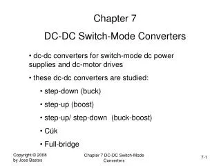
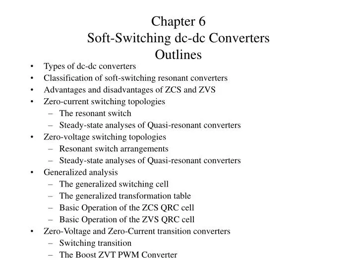
Chapter 6 Soft-Switching dc-dc Converters Outlines. Types of dc-dc converters Classification of soft-switching resonant converters Advantages and disadvantages of ZCS and ZVS Zero-current switching topologies The resonant switch Steady-state analyses of Quasi-resonant converters

E N D
Chapter 6Soft-Switching dc-dc ConvertersOutlines • Types of dc-dc converters • Classification of soft-switching resonant converters • Advantages and disadvantages of ZCS and ZVS • Zero-current switching topologies • The resonant switch • Steady-state analyses of Quasi-resonant converters • Zero-voltage switching topologies • Resonant switch arrangements • Steady-state analyses of Quasi-resonant converters • Generalized analysis • The generalized switching cell • The generalized transformation table • Basic Operation of the ZCS QRC cell • Basic Operation of the ZVS QRC cell • Zero-Voltage and Zero-Current transition converters • Switching transition • The Boost ZVT PWM Converter
Types of dc-dc Converters • The linear power supplies offer the designer four major advantages: • Simplicity in design, no electrical noise in its output, fast dynamic response time, and low cost. Applications are limited due to several disadvantages: • The input voltage is at least two or three volts higher than the output voltage because it can only be used as a step down regulator, • Each regulator is limited to only one output, and • Low efficiency when compared to other switching regulators • High frequency pulse width modulation (PWM) switching regulator circumvents all the linear regulators’ shortcomings: • Higher efficiency (68% to 90%) • Power transistors operate at their most efficient points • Multi-output applications are possible • Size and the cost are much lower • PWM switching converters still have several limitations • Greater circuit complexity compared to the linear power supplies • High Electromagnetic Interference (EMI) • Switching speeds below 100kHz because of high stress levels on power semiconductor devices
The Resonance Concept • Like switch mode dc-to-dc converters, resonant converters are used to convert dc-to-dc through an additional conversion stage: the resonant stage. • Advantages • natural commutation of power switches • low switching power dissipation • reduced component stresses, which in turn results in an increased power efficiency and an increased switching frequency • higher operating frequencies result in reduced size and weight of equipment and results in faster responses; hence, a possible reduction in EMI problems
Fig 6.1 Typical block diagram of soft-switching dc-to-dc converter • From a circuit standpoint, a dc-to-dc resonant converter can be described by three major circuit blocks • The dc-to-ac input inversion circuit, the resonant energy buffer tank circuit, and the ac-to-dc output rectifying circuit • The resonant tank serves as an energy buffer between the input and the output is normally synthesized by using a lossless frequency selective network • The ac-to-dc conversion is achieved by incorporating rectifier circuits at the output section of the converter
Resonant versus Conventional PWM • In PWM converters, the switching of semiconductor devices normally occurs at high current levels. • Therefore, when switching at high frequencies these converters are associated with high power dissipation in their switching devices. • Furthermore, the PWM converters suffer from EMI caused by high frequency harmonic components associated with their quasi-square switching current and/or voltage waveforms • In the resonant techniques, the switching losses in the semiconductor devices are avoided due to the fact that current through or voltage across the switching device at the switching point is equal to or near zero. • Compared to the PWM converters, the resonant converters show a promise of achieving the design of small size and weight converters • Another advantage of resonant converters over PWM converters is the decrease of the harmonic content in the converter voltage and current waveforms.
Classification of soft-Switching Resonant Converters • Quasi-resonant converters (single-ended) • Zero-current switching (ZCS) • Zero-voltage switching (ZVS) • Full-resonance converters (conventional) • Series resonant converter (SRC) • Parallel resonant converter (PRC) • Quasi-squarewave (QSW) converters • Zero-current switching (ZCS) • Zero-voltage switching (ZVS) • Zero-clamped topologies • Zero-clamped-voltage (CV) • Zero-clamped-current (CC) • Class E resonant converters • Dc link resonant inverters • Multi-resonant converters • Zero-current switching (ZCS) • Zero-voltage switching (ZVS) • Zero Transition Topologies • Zero-voltage transition (ZVT) • Zero- current transition (ZCT)
Advantages and Disadvantages of ZCS and ZVS • Power switch is turned ON and OFF at Zero-Voltage and Zero-Current • In ZCS topologies, the rectifying diode has ZVS • ZVS topologies, the rectifying diode has ZCS • Both the ZVS and the ZCS utilize transformer leakage inductances and diode junction capacitors and the output parasitic capacitor of the power switch. • Major disadvantage of the ZVS and ZCS techniques is that they require variable-frequency control to regulate the output • In ZCS, the power switch turns-OFF at zero current but at turn-ON, the converter still suffers from the capacitor turn-ON loss caused by the output capacitor of the power switch.
Switching Loci • Typical switching loci for a hard-switching converter without and with a snubber circuit as shown in Fig. 6.2. (a) (b) Fig 6.2 Switching loci. (a) Without snubber circuit. (b) With snubber circuit.
Switching Losses • There are two types of switching losses: • At turn-off, the power transformer leakage inductance produces high di/dt, which results in a high voltage spike across it • At turn-on, the switching loss is mainly caused by the dissipation of energy stored in the output parasitic capacitor of the power switch (a) (b) (a) (b) Fig 6.3 (a) ZVS at turn-on. (b) ZCS at turn-off. Fig 6.4 Typical switching current, voltage, and power loss waveforms at (a) turn-off and (b) turn-on.
Zero-Current Switching TopologiesThe Resonant Switch • Depending on the inductor-capacitor arrangements, there are two possible types of resonant switch arrangements • The switch is either an L-type or an M-type and can be implemented as a half-wave or a full-wave, i.e. unidirectional or bi-directional • LC tank forms the resonant tank that causes ZCS to occur (a) (a) (c) (b) (b) (c) Fig 6.6 Resonant switch. (a) M-type switch. (b) Half-wave implementation. (c) Full-wave implementation. Fig 6.5 Resonant switch. (a) L-type switch. (b) Half-wave implementation. (c) Full-wave implementation.
Steady-State Analysis of Quasi-Resonant Converters • To simplify the steady-state analysis • The filtering components , Lin, LF and Co are large when compared to the resonant components L and C • The output filter - Co - R is treated as a constant current source Io • The output filter Co - R is treated as a constant voltage source Vo • Switching devices and diodes are ideal • Reactive circuit components are ideal (a) (b) (c) Fig 6.7 Conventional converters: (a) buck, (b) boost, and (c) buck-boost
The Buck Resonant Converter • Replacing the switch by the resonant-type switch, to obtain a quasi-resonant PWM buck converter • It can be shown that there are four modes of operation under the steady-state condition (a) (b) Fig 6.8 (a) Conventional buck converter with L-type resonant switch. (b) Simplified equivalent circuit.
Buck Converter: Equivalent Modes (a) (b) (c) (d) Fig 6.9 (a) Equivalent circuit for Mode I. (b) Equivalent circuit for mode II. (c) Equivalent circuit for mode III. (d) Equivalent circuit for mode IV.
Buck Converter: Steady-State Analysis Mode I [ 0 t t1] • Mode I starts at t = 0 when S is turned ON • Assume for t > 0, both S and D are ON • The capacitor voltage, vc , is zero and the input voltage is equal to the inductor voltage • The inductor current, iL, is given by • As long as the inductor current is less than Io, the diode will continue conducting and the capacitor voltage remains at zero. (6.3) • Hence, the time interval = t1 is given by (6.4) • This is the inductor current charging state.
Steady-State Analysis (cont’d) Mode II [t1 t t2] • Mode II starts at t1, diode is open resonant stage between L and C • The first-order differential equations that represent this mode are (6.5a) (6.5b) • Inductor current is given by (6.6) • The general solution for iL(t) is given by (6.7) • Resonant angular frequency and constants: • A2 to equal, A3 = Io
Steady-State Analysis (cont’d) Equations iL and vc are given by (6.8) (6.9) is known as the characteristic impedance The time interval in this mode can be derived at t = t2 by setting iL(t2) = 0, (6.10) therefore, (6.11) Mode III starts at t = t, when the switch is turned OFF.
Steady-State Analysis (cont’d) Mode III [t2 t t3]: At t2, the inductor current becomes zero, and the capacitor linearly discharges from (t2) to zero during t2 to t3. The capacitor current equals to as given by, (6.12) The capacitor voltage vc(t) is obtained from Eq. (6.12) from t2 to t with as the initial value, (6.13) The initial value (t2) is obtained from previous mode, (6.14) Substituting Eq. (6.14) into Eq. (6.13), (6.15) At t = t3, the capacitor voltage becomes zero, (6.16) At this point, the diode turns ON and the circuit enters Mode IV.
Steady-State Analysis (cont’d) Mode IV [t3 t t4]: At this mode the switch remains OFF, but the diode starts conducting at t = t3. Mode IV continues as long as the switch is OFF, and the output current starts the free-wheeling stage through the diode. Initial conditions By turning ON the switch at t = , the cycle repeats these four modes. The dead time is given by, (6.17)
Typical Steady-State Waveforms Voltage Gain The expression for the voltage gain, Figure 6.10 shows the steady state waveforms for and for the buck converter with L-type switch. Fig 6.10 Steady-state current and voltage waveforms of buck L-type
Voltage Gain Substitute for vc(t) from intervals (t2-t1) and (t3-t2), to yield, (6.18) The voltage gain ratio is given by, (6.19) Substitute for (t2-t1), (t3-t2) and VC(t2) from the above modes, a closed form expression for M in terms of the circuit parameters can be obtained.
Voltage Gain (cont’d) The total input energy over one switching cycle, (6.20) Since is equal to , Eq. (6.20) is rewritten as, (6.21) Substituting for iL(t) from Eqs. (6.2) and (6.8) into the above integrals, Eq. (6.21) becomes, (6.22) Substituting for (6.23) with, ,Eq. (6.23) becomes, (6.24)
Voltage Gain (cont’d) The output energy over one switching cycle is: (6.25) Equating the input and output energy expressions (6.26) From Eq. (6.26) the voltage gain is expressed by, (6.27) Substituting for t1, (t2-t1) and (t3-t2) from previous equations, the voltage gain becomes (6.28)
Normalization To simplify and generalize the gain equation, the following normalized parameters are defined: normalized output voltage (6.29a) (6.29b) normalized load (6.29c) average output current (6.29d) normalized switching frequency By substituting Eq. (6.29) into Eq. (6.28), the final voltage gain is simplified into (6.30) where, (6.31)
Buck-Control Characteristic Curve A plot of the control characteristic curve of M vs. fns under various normalized loads is given in Fig. 6.11 Fig 6.11 Control characteristic curve of M vs. ns for the ZCS buck converter.
ZCS Buck Converter Example 6.1 Consider the following specifications for a ZCS buck converter of Fig. 6.8(a). Assume the parameters are: Vin = 25V, Vo = 12V, Io = 1A, fs = 250kHz Design for the resonant tank parameters L and C and calculate the peak inductor current, and peak capacitor voltage. Determine the time interval for each mode. Solution: The voltage gain is . Select . Determine Q from either the control characteristic curve of Fig. 6.11 or from the gain equation of Eq. (6.30). This results in Q approximately equaling 1. Since , the characteristic impedance is given by, The second equation in terms of L and C is obtained from fo. From the normalized switching frequency, fo may be given by, (6.32) In terms of the angular frequency, o, (6.33) Solving Eqs. (6.32) and (6.33) for L and C, we obtain,
Example 6.1 (cont’d) The peak inductor current, is given by, The peak capacitor voltage is: The time intervals are calculated from the following expressions: For t’max we have
The ZCS Boost Converter The boost-quasi-resonant converter with an M-type switch as shown in Fig. 6.13(a), with its equivalent circuit shown in Fig. 6.13(b). (a) (b) Fig 6.13 (a) ZCS boost converter with M-type switch. (b) Simplified equivalent circuit.
ZCS Boost Converter: Steady-State Analysis Mode I [ 0 t t1]: Assume switch and the diode are both ON The output voltage is given by The initial inductor current and capacitor voltage, Integrating Eq. (6.34), the inductor current becomes, When the resonant inductor current reaches the input current, , the diode turns OFF, with t1 given by, At t = t1, the diode turns OFF since = , and the converter enters Mode II.
Steady-State Analysis (cont’d) Mode II [t1 t t2]: The switch remains closed, but the diode is OFF at tin Mode II as shown in Fig. 6.14(b). This is a resonant mode during which the capacitor voltage starts decreasing resonantly from its initial value of . When = , the capacitor reaches its negative peak. At t = t2, equals zero, and the switch turns OFF, hence, switching at zero-current. The initial conditions, From Fig. 6.14(b), the first derivatives for iL and vc are, Using the same solution technique used in the buck converter to solve the above differential equations, the expression for iL(t) (6.37) (6.38) where At , and the time interval can be obtained from evaluating Eq. (6.37) at to yield, (6.39)
Fig 6.14 (a) Equivalent circuit for mode I. (b) Equivalent circuit for mode II. (c) Equivalent circuit for mode III. (d) Equivalent circuit for mode IV. ZCS Boost: Equivalent Circuit Modes (a) (b) (c) (d)
Steady-State Analysis (cont’d) Mode III [t2 t t3]: Mode III starts at t, and the switch and the diode are both open as shown in Fig. 6.14(c). Since is constant, the capacitor starts charging up by the input current source. The capacitor voltage, (6.40) The diode begins conducting at when the capacitor voltage is equal to the output voltage, i.e. vc(t3)=Vo. Time interval in this period (6.41) Mode IV [t3 t t4]: At t3, the capacitor voltage is clamped to the output voltage, and the diode starts conducting again. The cycle of the mode will repeat again at the time of when S is turned ON again
Steady-State Analysis (cont’d) Mode IV [t3 t t4]: At t3, the capacitor voltage is clamped to the output voltage, and the diode starts conducting again. The cycle of the mode will repeat again at the time of when S is turned ON again
ZCS Boost-Typical Steady-State Waveforms Typical steady state waveforms are shown in Fig. 6.15. Fig 6.15 Steady-state waveforms of the boost converter with M-type switch.
ZCS Boost Converter Voltage Gain Conservation of energy per switching cycle to express the voltage gain, The input energy is, (6.42) The output energy, (6.43) The output current equals io=Iin-iL and io=Iin for intervals 0tt1 and t3t<Ts,, (6.44) The input current is obtained from the conservation of output power as:
ZCS Boost-Voltage Gain Substituting for the input current and by evaluating Eq. (6.44), the output energy becomes (6.45) with and , and use the equations for . and from Eqs. (6.39) and (6.41), Eq. (6.45) becomes, (6.46) The voltage gain expression is given by, (6.47) where, , M, Io and fns are given as before.
ZCS Boost-Control Characteristic Curve Fig 6.16 shows the characteristic curve for M vs. as a function of the normalized load. Fig 6.16 Characteristic curve for M vs. ns for the boost ZCS converter.
ZCS Boost Converter Example 6.2 Design a boost ZCS converter for the following parameters: Vin = 20V, Vo = 40V. Po =20W, fs = 250kHz. Solution: The voltage gain is .Let us select . From the characteristic curve of Fig. 6.16, Q can be approximated to 6.0 The characteristic impedance is given by, (6.48) Resonant frequency is, (6.49) Solve Eqs. (6.48) and (6.49) for L and C To limit the input ripple current and the output voltage, we select,
ZCS Boost Converter Example 6.3 Design a boost converter with ZCS, with the following design parameters: Vin=25V, P0=30W at I0=0.5A, and fs=100kHz. Assume the output voltage ripple Solution: From the characteristic curve of Fig. 6.15, approximate Q to 6 when we assume fn = 0.58. From Q and Ro, the characteristic impedance is obtained from, Solving for C and L From obtained from the ripple voltage equation for the conventional boost converter, which is given by,
Example 6.3 (cont’d) The time intervals are given by
Other ZCS Boost Converter Figure 6.17(a) shows the quasi-resonant boost converter by using the L-type resonant switch, and the simplified circuit and its steady state waveforms are shown in Fig.6. 17(b) and (c), respectively. (b) (c) (a) Fig 6.17 (a) ZCS boost converter with L-type switch. (b) Simplified equivalent circuit. (c) Steady-state waveforms.
ZCS Buck-boost Converter Quasi-resonant buck-boost converter by using the L-type switch as shown in Fig. 6.18(a), Fig. 6.18(b) shows the simplified equivalent circuit. (b) (a) Fig 6.18 (a) ZCS buck-boost converter with L-type switch. (b) Simplified equivalent circuit.
ZCS Buck-Boost Converter-Steady-State Analysis The Buck-boost converter also leads to four modes of operations. Mode I [ 0 t t1]: Mode I starts at t = 0, the switch and the diode are both conducting. According to Kirchhoff’s law, the voltage equation can be written as (6.50) By integrating both sides of Eq. (6.50) with the initial condition of , is given by, (6.51) and At t = t1, the inductor current reaches IF, forcing the output diode to stop conducting, so t1 can be express as, (6.52)
Steady-State Analysis (cont’d) Mode II [t1 t t2]: This is a resonant stage between L and C with the initial conditions given by Applying Kirchhoff’s law, in Fig. 6.19(b), the inductor current and capacitor voltage equations may be given as (6.53a) (6.53b) Solving Eqs. (6.53) for t > t, (6.54) (6.55) At ,the inductor current reaches zero, ,and the switch stops conducting. The time interval is given by, (6.56)
Steady-State Analysis (cont’d) Mode III [t2 t t3]: Mode III starts at t = t2 when the inductor current reaches zero. The switch and the diode are both OFF. The capacitor starts to discharge until it reaches zero, and the diode will start to conduct again at t = t3. During this period, the inductor current is zero. The diode begins to conduct at the end of this mode, , because the capacitor voltage is equal to zero where may be obtained from Eq. (6.55) by evaluating it at t = t2. The expression from Eq. (6.57) for the time between t2 and t3 is, Mode IV [t3 t t4]: Between t3 and t4, the switch remains OFF, but the diode is ON. At the end of the cycle, the switch is closed again when the current is zero. The cycle of the modes will repeat again at Ts.
ZCS Buck-Boost Converter-Equivalent Circuit Modes (a) (b) (c) (d) Fig 6.19 (a) Equivalent circuit for mode I. (b) Equivalent circuit for mode II. (c) Equivalent circuit for mode III. (d) Equivalent circuit for mode IV.
ZCS Buck-Boost Converter – Typical Steady-State Analysis The steady state waveforms shown in Fig. 6.20 are the characteristic waveforms for the switch, , and . Fig 6.20 Steady-state waveforms for buck-boost converter with L-type switch.
ZCS Buck-Boost Converter Voltage Gain • Conservation of energy per switching cycle will be used as before to obtain the voltage gain, • The buck-boost-ZCS converter gain is given by (6.59) Fig 6.21 Characteristic curve for M vs. ns for the ZCS buck-boost converter.
Example 6.4 Consider a buck-boost QRC-ZCS converter with the following specifications: Vin=40V, Po=80W at Io=4A, fs=250kHz, Lo=0.1mH, and Co=6 F. Design values for L and C and determine the output ripple voltage. Solution: The output voltage and load resistance are given by The voltage gain is given by With M = 0.5, and fns= 0.17, we select , to yield, From Q, and Z0, and From the above equation C and L are given by, The duty cycle D is approximately 33% since the voltage gain for the buck-boost is 0.5. Hence, the voltage ripple is,
ZERO-Voltage Switching Topologies • The Zero-Voltage-Switching (ZVS) Quasi-resonant converter family. Like the ZCS topologies, M-type or L-type switch arrangements can be used. • The power switch is turned ON at zero-voltage (of course the turn OFF also occurs at zero-voltage). • A flyback diode across the switch (body diode) is used to damp the voltage across the capacitor
Switch Implementation Figure 6.23(a) shows a MOSFET switch implementation by including an internal body diode and a parasitic capacitance. We will assume and are too small to be included. If the body diode is not fast enough for the designed application or has limited power capabilities, it is practically possible to block it and use an external, fast flyback diode as shown in Fig. 6.23(b). is used to block , and is the actual diode used to carry the reverse switch current. (a) (b) Fig 6.23 (a) MOSFET implementation. (b) MOSFET switch with fast flyback diode.