Download
1 / 44
600 likes | 893 Views
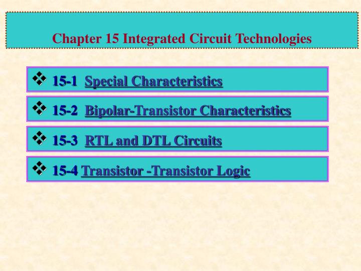
Chapter 15 Integrated Circuit Technologies. 15-1 Special Characteristics. 15-2 Bipolar-Transistor Characteristics. 15-3 RTL and DTL Circuits. 15-4 Transistor -Transistor Logic. Chapter 15 Integrated Circuit Technologies. 15-5 Emitter-Coupled Logic.

E N D
Chapter 15 Integrated Circuit Technologies • 15-1 Special Characteristics • 15-2 Bipolar-Transistor Characteristics • 15-3 RTL and DTL Circuits • 15-4 Transistor -Transistor Logic
Chapter 15 Integrated Circuit Technologies • 15-5 Emitter-Coupled Logic • 15-6 Metal-Oxide Semiconductor (MOS) • 15-7 Complementary MOS (CMOS) • 15-8 CMOS Transmission Gate Circuits
15-1 Special Characteristics Fan-Out The fan-out of a gate specifies the number of standard loads that can be connected to the output of the gate without degrading its normal operation. The fan-out is calculated from the amount of current available in the output of a gate and the amount of current needed in each input of a gate.
15-1 Special Characteristics Fan-Out The fan-out of the gate is calculated from the ratio IOH/IIH or IOL/IIL, whichever is smaller.
15-1 Special Characteristics Power Dissipation The power dissipation is a parameter that represents the amount of power needed by the gate. The current that is drawn from the power supply when the output of the gate is in the low-voltage level The current that is drawn from the power supply when the output of the gate is in the high-voltage level The power is the product VCC × ICC . The current drain from the power supply depends on the logic state of the gate. Supply voltage The current that is drawn by the circuit. The average current is ICC (avg) = ( ICCH + ICCL) /2
15-1 Special Characteristics Power Dissipation The average power dissipation PD (avg) = ICC (avg) × VCC In a typical digital system there will be many IC, and the power required by each IC must be considered. The total power dissipation in the system is the sum total of the power dissipated in the all ICs.
15-1 Special Characteristics Propagation Delay The propagation delay of a gate is the average transition-delay time for the signal to propagate from input to output when the binary signal changes in value. The signal-delay time between the input and output when the output changes from the high to the low level is referred to as tPHL
15-1 Special Characteristics Propagation Delay The propagation delay of a gate is the average transition-delay time for the signal to propagate from input to output when the binary signal changes in value. When the output goes from the low to the high level, the delay is tPLH
15-1 Special Characteristics Noise Margin Noise is a term used to denote an undesired signal that is superimposed upon the normal operating signal. Noise margin is the maximum noise voltage added to an input signal of a digital circuit that does not cause an undesirable change in the circuit output
Noise margin is the difference VOH -VIH or VIL -VOL , whichever is smaller. 15-1 Special Characteristics Noise Margin
C C o B i B E 15-2 Bipolar-Transistor Characteristics Demonstration Consider the inverter circuit of the figure with the following parameters: RC = 1kΩVCC = 5V RB = 22kΩVOH = 5V hFE = 50 VOL = 0.2 V
C C o B i B E 15-2 Bipolar-Transistor Characteristics Demonstration IB = (Vi – VBE) / RB = (5V – 0.7V) / 22kΩ = 0.195mA ICS = (VCC – VCE) / RC = (5V – 0.2V) /1kΩ = 4.8mA 0.195mA = IB≥ ICS/hFE= 4.8mA/50 =0.096mA Assuming VCE =0.2V The transistor is saturated and its output voltage VO = VCE =0.2V= L
15-3 RTL and DTL Circuit RTL Basic Gate If all inputs are low at 0.2 V, all transistors are cut off. This causes the output of the circuit to be high.
15-3 RTL and DTL Circuit RTL Basic Gate If any input of the RTL gate is high, the corresponding transistor is driven into saturation. This causes the output to be low, regardless of the states of the other transistors.
15-3 RTL and DTL Circuit DTL Basic Gates If any input of the gate is low at 0.2V, the corresponding input diode conducts current through VCCand the 5kΩresistor into the input node. The voltage of P is equal to a total of 0.9V that is not enough to overcome the a potential of one VBEdrop plus two diode drop. The transistor is cutoff. The output voltage is high at 5V.
15-3 RTL and DTL Circuit DTL Basic Gates If all inputs are high, the transistors is driven into the saturation region. This causes the output to be low.
CC 15-3 RTL and DTL Circuit DTL Basic Gates The fan-out of a DTL gate may be increased by replacing one of the diodes in the base circuit with a transistor.
15-4 Transistor -Transistor Logic The original basic TTL gate was a slight improvement over the DTL gate. TTL gates have three different types of output configuration: • Open-collector output • Totem-pole output • Three-state (or tristate) output
15-4 Transistor -Transistor Logic Open-Collector Output Gate The basic TTL gate is a modified circuit of the DTL gate.
15-4 Transistor -Transistor Logic Open-Collector Output Gate The basic TTL gate is a modified circuit of the DTL gate
15-4 Transistor -Transistor Logic Open-Collector Output Gate The basic TTL gate is a modified circuit of the DTL gate
15-4 Transistor -Transistor Logic Open-Collector Output Gate If any input is low, the voltage at the base of Q1 is equal to 0.9V. In order for Q3 to start conducting, the voltage at the the base of Q1 must be greater than 1.8V. 0.9V 0.2V 1.8V Therefore, the output transistor is cutoff.
15-4 Transistor -Transistor Logic Open-Collector Output Gate If all input are high, both Q2 Q3 conduct and saturate. The base voltage of Q1 is equal to the voltage across its base-collector pn junction plus two VBEdrop in Q2and Q3, or 2.1V. 2.1V 3V The output transistor saturates, the output goes low to 0.2V
15-4 Transistor -Transistor Logic Open-Collector Output Gate If the output of several open-collector TTL gates are tied together with a single external resistor, a wired-AND logic is performed. The wire-AND logic gives a high level only if all variables are high; otherwise, the function is low.
15-4 Transistor -Transistor Logic Open-Collector Output Gate The wire-AND gate is not a physical gate, but only a symbol to designate the function obtained from the indicated connection.
15-4 Transistor -Transistor Logic Open-Collector Output Gate Open-collector gates can be tied together to form a common bus. Three of the inputs are 0, which produces a 1 on the bus. The fourth input, I4, can now transmit information through the common-bus line into inverter 5.
Internal temperature and voltage compensated bias network C2 C1 EB P P P E P E 15-5 Emitter-Coupled Logic Differential input amplifier Emitter-follower outputs
15-5 Emitter-Coupled Logic The graphic symbol of ECL Gate Two outputs of two or more ECL gates can be connected together to form wired logic. Wired-OR Wired-AND
15-6 Metal-Oxide Semiconductor (MOS) Inverter • When the input voltage is low (below VT), Q2 turns off. The output voltage is at about VDD. • When the input voltage is high (above VT), Q2 turns on. The output voltage is at a voltage below VT.
15-6 Metal-Oxide Semiconductor (MOS) NAND Gate • Input A and B must both be high for all transistors to conduct and cause the output to go low. • If either input is low, the corresponding transistor is turned off and the output is high. 0 1 1
15-6 Metal-Oxide Semiconductor (MOS) NAND Gate • Input A and B must both be high for all transistors to conduct and cause the output to go low. • If either input is low, the corresponding transistor is turned off and the output is high. 1 0 1
15-6 Metal-Oxide Semiconductor (MOS) NOR Gate • If either input is high, the corresponding transistor conducts and the output is low. • If all inputs are low, all active transistors are off and the output is high.
15-7 Complementary MOS (CMOS) Inverter • When the input is low, both gates are zero potential. The input is at –VDD, relative to the source of the p-channel device and at 0 V relative to the source of the n-channel device. p-channel device is turned on and the n-channel device is turned off. The source terminal of the p-channel device is at VDD 1 0 The source terminal of the n-channel device is at ground.
15-7 Complementary MOS (CMOS) Inverter 2. When the input is high, both gates are at VDD. The p-channel device is turned off and the n-channel device is turned on. 0 1
15-7 Complementary MOS (CMOS) NAND Gate A two-input NAND gate consists of two p-type units in parallel and two n-type units in serial. 0 1 If all inputs are high, both p-channel transistors turn off and both n-channel transistors turn on. The output produces a low state. 1
15-7 Complementary MOS (CMOS) NAND Gate If any input is low, the associated n-channel transistor is turned off and the associated p-channel transistor is turned on. The output goes to the high state. 1 1 0
15-7 Complementary MOS (CMOS) NOR Gate A two-input NOR gate consists of two n-type units in parallel and two p-type units in serial. 0 0 1 If all inputs are low, both p-channel transistors turn on and both n-channel transistors turn off. The output goes to the high state.
15-7 Complementary MOS (CMOS) NOR Gate If any input is high, the associated p-channel transistor is turned off and the associated n-channel transistor is turned on. The output goes to the low state. 1 0 0
15-7 Complementary MOS (CMOS) COMS Characteristics • Low power dissipation • Greater packing density • Good noise immunity • Reasonable propagation delay
15-8 CMOS Transmission Gate Circuits A transmission gate consists of one n-channel and one p-channel MOS transistor connected in parallel. 0 When the N gate is at ground and Pgate at VDD, both transistors are off and there is an open circuit between X and Y. 1
15-8 CMOS Transmission Gate Circuits When the N gate is at VDD and Pgate at ground, both transistors are on and there is an close circuit between X and Y. 1 0 The block diagram of the transmission gate
15-8 CMOS Transmission Gate Circuits The transmission gate is usually connected to an inverter and referred to as a bilateral switch. • When C=1, the switch is closed; • when C=0, the switch is open.
15-8 CMOS Transmission Gate Circuits The block diagram of Exclusive-OR Constructed with Transmission Gates Exclusive-OR Constructed with Transmission Gates The truth table of Exclusive-OR Constructed with Transmission Gates