Download

1 / 32
330 likes | 493 Views
Basic Resistive Load Circuits. Dr. Paul Hasler. V dd. V dd = 5.0V. GND. What is the bias current?. I ref = (2V) / R 1. Basic Resistive Load Circuits. Output Voltage Bias = 3.0V. R 1. R 1. V out. V out. V in. V in. GND. V dd. V dd = 5.0V. GND. Basic Resistive Load Circuits.

E N D
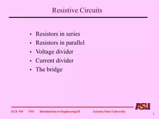
Basic Resistive Load Circuits Dr. Paul Hasler
Vdd Vdd= 5.0V GND What is the bias current? Iref = (2V) / R1 Basic Resistive Load Circuits Output Voltage Bias = 3.0V R1 R1 Vout Vout Vin Vin GND
Vdd Vdd= 5.0V GND Basic Resistive Load Circuits Output Voltage Bias = 3.0V R1 R1 Iref = (2V) / R1 Vout Vout Vin Vin GND BJT / Subthreshold VT Above Threshold (Vd > Vg - VT ) (2V) / R1 = (K/2) (Vin - VT )2 (2V) / R1 = Ico eVin/UT Vin = VT + sqrt( (4V) / (K R1) ) Vin = UT ln ( (2V) / R1 Ico )
Vdd Vdd= 5.0V GND Small-Signal Model: Common Drain Output Voltage Bias = 3.0V R1 R1 Iref = (2V) / R1 Vout Vout Have bias Vin Vin Vin GND
V3 + V - V1 rp gmV ro V2 V2 Small-Signal Modeling V3 V3 I I V1 V1 V2 V2 rp gm ro Av BJT (UTb) / I I / UT VA / I VA / UT Above VT MOSFET 2I /(V1-V2 -VT) VA / I 2VA/(V1-V2 -VT) Sub VT MOSFET kI / UT VA / I kVA / UT
Vdd Vdd= 5.0V GND Small-Signal Model: Common Drain Output Voltage Bias = 3.0V R1 R1 Iref = (2V) / R1 Vout Vout Have bias Vin Vin Vin GND Compute Transconductance (gm) BJT / Subthreshold VT Above Threshold (Vd > Vg - VT ) gm = 2I /(Vin -VT) = (4V) / (R1 (Vin -VT) ) gm = I / UT = (2V) / (R1 UT)
Vdd Vdd= 5.0V GND GND Vin Vout + V - gmV R1 rp Small-Signal Model: Common Drain Output Voltage Bias = 3.0V Iref = (2V) / R1 R1 R1 Have bias Vin Vout Vout gm = (2V) / (R1 UT) Vin Vin or GND gm = (4V) / (R1 (Vin -VT) ) Gain = - gmR1 = - [ (2V) /(R1UT) ] R1 = - (2V) /UT or Gain = -(4V) / (Vin -VT)
Vdd Vdd= 5.0V GND GND Small-Signal Model: Common Drain Output Voltage Bias = 3.0V Iref = (2V) / R1 R1 R1 Have bias Vin Vout Vout gm = (2V) / (R1 UT) Vin Vin or GND gm = (4V) / (R1 (Vin -VT) ) Vout Vin Gain = - [(2V) / UT ][1 + (2V)/ VA ] + V - or gmV R1 rp ro Gain = -[(4V)/(Vin -VT)][1 + (2V)/ VA ]
Vdd Vdd= 5.0V GND GND Vin Vout + V - gmV R1 rp Small-Signal Model: Common Drain Output Voltage Bias = 3.0V Iref = (2V) / R1 R1 R1 Have bias Vin Vout Vout gm = (2V) / (R1 UT) Vin Vin or GND gm = (4V) / (R1 (Vin -VT) ) Gain = - (2V) /UT or Gain = -(4V) / (Vin -VT) Output Resistance = R1
Vdd What is the bias current? Iref = (3V) / R1 Follower Circuits Vdd Output Voltage Bias = 3.0V Vin Vin Vout Vout R1 R1 GND GND
Vdd Basic Resistive Load Circuits Vdd Output Voltage Bias = 3.0V Vin Vin Vout Vout Iref = (3V) / R1 R1 R1 GND GND BJT / Subthreshold VT Above Threshold (Vd > Vg - VT ) (3V) / R1 = (K/2) (Vin - Vout - VT )2 (3V) / R1 = Ico e(Vin - Vout)/UT Vin = Vout + VT + sqrt((6V)/(KR1)) Vin = Vout + UT ln ( (3V) / R1 Ico )
Vdd Vin Vin Vout Vout R1 R1 GND Vdd GND Small-Signal Model: Common Drain Output Voltage Bias = 3.0V Iref = (3V) / R1 Have bias Vin Compute Transconductance (gm) BJT / Subthreshold VT Above Threshold (Vdd > Vin - VT ) gm = 2I /(Vin –3V - VT) = (6V) / (R1 (Vin - 3V- VT) ) gm = I / UT = (3V) / (R1 UT)
Vdd Vin Vin Vout Vout R1 R1 GND Vdd GND GND GND Small-Signal Model: Common Drain Output Voltage Bias = 3.0V Iref = (3V) / R1 Have bias Vin gm = (3V) / (R1 UT) or gm = (6V) / (R1 (Vin-3V-VT) ) + V - (Vin - Vout ) / rp + (Vin - Vout ) gm = Vout / R1 Vin Vout rp R1 gmV (Vin-Vout )(1 + rp gm) = Vout (rp / R1) Vout/Vin = 1/(1 + [(rp / R1)/(1 + rp gm)])
Vdd Vin Vin Vout Vout R1 R1 GND Vdd GND GND GND Small-Signal Model: Common Drain Output Voltage Bias = 3.0V Iref = (3V) / R1 Have bias Vin gm = (3V) / (R1 UT) or gm = (6V) / (R1 (Vin-3V-VT) ) + V - Vout / Vin = 1 / (1 + [ (rp / R1) / (1 + rp gm)]) Vin Vout rp R1 rp gm = b (large) gmV Vout / Vin = 1 / ( 1 + [ 1 / (R1 gm)] )
Vdd Vin Vin Vout Vout R1 R1 GND Vdd GND GND GND Small-Signal Model: Common Drain Output Voltage Bias = 3.0V Iref = (3V) / R1 Have bias Vin gm = (3V) / (R1 UT) or gm = (6V) / (R1 (Vin-3V-VT) ) + V - Vout / Vin = 1 / (1 + [ 1 / (R1 gm)]) Vin Vout rp Vout / Vin = 1 / (1 + [UT/(3V)]) R1 gmV or Vout / Vin = 1 / (1 + [Vin-3V-VT /(3V)])
Vdd Vin Vin Vout Vout R1 R1 GND Vdd GND GND GND Small-Signal Model: Common Drain Output Voltage Bias = 3.0V Iref = (3V) / R1 Have bias Vin gm = (3V) / (R1 UT) or gm = (6V) / (R1 (Vin-3V-VT) ) + V - Vout/Vin = 1/(1 + [UT/(3V)]) or Vin Vout rp Vout/Vin = 1/(1+[Vin-3V-VT /(3V)]) R1 gmV Output Resistance: Short the input to GND
Vdd Vin Vin Vout Vout R1 R1 GND Vdd GND GND GND GND Small-Signal Model: Common Drain Output Voltage Bias = 3.0V Iref = (3V) / R1 Have bias Vin gm = (3V) / (R1 UT) or gm = (6V) / (R1 (Vin-3V-VT) ) Vout/Vin = 1/(1 + [UT/(3V)]) Vout or Vout/Vin = 1/(1+[Vin-3V-VT /(3V)]) 1/gm rp R1 Rout = (1/gm) / (1 + gm R1) ~ 1/gm
Vdd Vdd What is the bias current? Iref = (1V) / R1 Common Gate: Resistive Load Output Voltage Bias = 4.0V R1 R1 Vout Vout Vb Vb Vin Vin
Vdd Vdd Common Gate: Resistive Load Output Voltage Bias = 4.0V R1 R1 Iref = (1V) / R1 Vout Vout Vb Vb Vin Vin BJT / Subthreshold VT Above Threshold (Vd > Vg - VT ) (1V) / R1 = Ico eVb-Vin/UT (1V) / R1 = (K/2) (Vb - Vin - VT )2 Vin = Vb - VT - sqrt((2V)/(K R1)) Vin = Vb - UT ln ( (1V) / R1 Ico )
Vdd Vdd Common Gate: Small-Signal Output Voltage Bias = 4.0V R1 R1 Iref = (1V) / R1 Vout Vout Have Input Bias Vb Vb Vin Vin BJT / Subthreshold VT Above Threshold (Vd > Vg - VT ) gm = 2I /(Vb - Vin -VT) = (2V) / (R1 (Vb - Vin -VT) ) gm = I / UT = (1V) / (R1 UT)
Vdd Vdd GND GND Common Gate: Small-Signal Output Voltage Bias = 4.0V R1 R1 Iref = (1V) / R1 Vout Vout Have Input Bias Vb gm = (1V) / (R1 UT) Vb or Vin Vin gm = (2V) / (R1(Vb- Vin-VT) ) Vout Gain = gm R1 + V - R1 rp Gain = (1V) / UT gmV or Vin Gain = (2V) / (Vb- Vin-VT)
Vdd Vdd GND GND Common Gate: Small-Signal Output Voltage Bias = 4.0V R1 R1 Iref = (1V) / R1 Vout Vout Have Input Bias Vb gm = (1V) / (R1 UT) Vb or Vin Vin gm = (2V) / (R1(Vb- Vin-VT) ) Vout Gain = (1V) / UT or Gain = (2V) / (Vb- Vin-VT) + V - R1 rp gmV Vin Output Resistance = R1
Modify gm Vdrain Source Degeneration Vdrain Vin Vin Va Va R1 R1 GND GND
Vdd GND GND Small-Signal Model: Common Drain Vdd + V - Vin Vin Vin Vout Vout rp Vout R1 gmV R1 R1 GND GND Vout / Vin = 1 / ( 1 + [ 1 / (R1 gm)] ) = R1 gm / (1 + R1 gm) R1 << 1/gm R1 >> 1/gm Vout / Vin = (R1 gm) Vout / Vin ~ 1 (Resistor has a small effect) (Resistor sets gm)
Modify gm Vdrain GND R1gm << 1 gm = Vin 1 + R1gm R1gm >> 1 Source Degeneration Vdrain Vdrain ro + V - Vin Vin Vin Va Va Va rp R1 R1 R1 gmV Vdrain GND GND R1 gm Gm: gmV = gm(Vin - Va ) = gm(1 - ) Vin 1 + R1gm (ignore ro here) gmVin Vin /R
Vdrain ro + V - Va rp Modify gm R1 gmV Vdrain Vdrain GND GND Source Degeneration Vdrain Vin Vin Va Va R1 R1 GND GND Gm = 1/R Rout:
Modify gm Vdrain GND small small Source Degeneration Vdrain Vdrain Vdrain gmVa ro Vin Vin Va Va Va rp // R1 R1 R1 GND GND Gm = 1/R Solve for Va: Va / (rp // R1) + gmVa = (Vdrain - Va)/ ro Rout: Va [ro (gm+ (1/(rp // R1)) )] = Vdrain Va = Vdrain /[rogm]
Modify gm Vdrain GND Source Degeneration Vdrain Vdrain Vdrain gmVa ro Vin Vin Va Va Va rp // R1 R1 R1 GND GND Va = Vdrain /[rogm] Gm = 1/R Solve for Current: I = Va / (rp // R1) Rout: I = Vdrain /[rogm(rp // R1)] Rout = rogm(rp // R1)
Modify gm Rin bR1 Vin Vdrain Vdrain small GND Source Degeneration Rin: (conductance is zero for a MOSFET) Vdrain Vin Vin “Reflect R1 through the base” Va Va R1 R1 GND GND Gm = 1/R Rout = rogm(rp // R1) Rin = bR1 + rp = b R1(1 + (1/(gmR1) ) ) Rin = b R1
Modify gm Vdrain GND Source Degeneration Vdrain Vin Vin Vin Vdrain + V - Va Va GmV Rin Rout R1 R1 GND GND Gm = 1/R Voltage Gain: Gm Rout = rogm(1 // (R1/rp ) ) Rout = rogm(rp // R1) Rin = b R1