Download
1 / 1
10 likes | 148 Views
Optical Chemical Sensor Systems based on Photosensitive Hybrid Sol-Gel Glass B.D. MacCraith, S. Aubonnet, H. Barry, C. von Bültzingslöwen, J.-M. Sabattié, C.S. Burke Optical Sensors Laboratory - National Centre for Sensor Research Dublin City University - Ireland. 1 Introduction

E N D
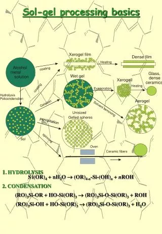
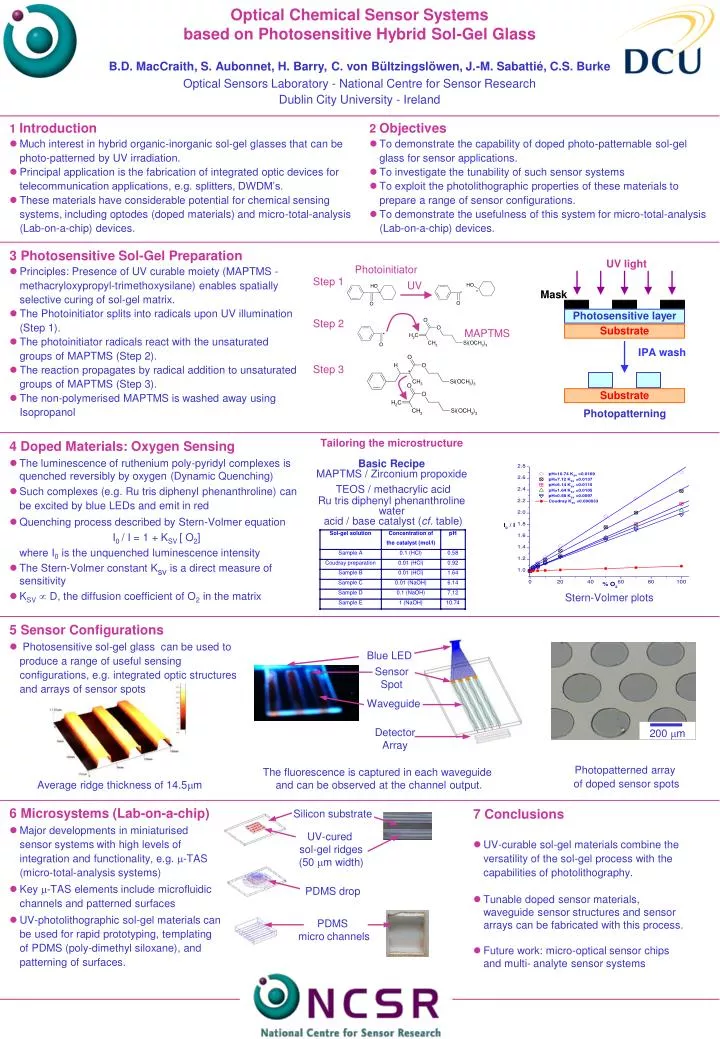
Optical Chemical Sensor Systems based on Photosensitive Hybrid Sol-Gel Glass B.D. MacCraith, S. Aubonnet, H. Barry, C. von Bültzingslöwen, J.-M. Sabattié, C.S. Burke Optical Sensors Laboratory - National Centre for Sensor Research Dublin City University - Ireland • 1 Introduction • Much interest in hybrid organic-inorganic sol-gel glasses that can be photo-patterned by UV irradiation. • Principal application is the fabrication of integrated optic devices for telecommunication applications, e.g. splitters, DWDM’s. • These materials have considerable potential for chemical sensing systems, including optodes (doped materials) and micro-total-analysis (Lab-on-a-chip) devices. • 2 Objectives • To demonstrate the capability of doped photo-patternable sol-gel glass for sensor applications. • To investigate the tunability of such sensor systems • To exploit the photolithographic properties of these materials to prepare a range of sensor configurations. • To demonstrate the usefulness of this system for micro-total-analysis (Lab-on-a-chip) devices. • 3 Photosensitive Sol-Gel Preparation • Principles: Presence of UV curable moiety (MAPTMS - methacryloxypropyl-trimethoxysilane) enables spatially selective curing of sol-gel matrix. • The Photoinitiator splits into radicals upon UV illumination (Step 1). • The photoinitiator radicals react with the unsaturated groups of MAPTMS (Step 2). • The reaction propagates by radical addition to unsaturated groups of MAPTMS (Step 3). • The non-polymerised MAPTMS is washed away using Isopropanol Photoinitiator Step 1 Mask Photosensitive layer Step 2 Substrate MAPTMS UV light IPA wash Step 3 UV Substrate Photopatterning 4 Doped Materials: Oxygen Sensing • The luminescence of ruthenium poly-pyridyl complexes is quenched reversibly by oxygen (Dynamic Quenching) • Such complexes (e.g. Ru tris diphenyl phenanthroline) can be excited by blue LEDs and emit in red • Quenching process described by Stern-Volmer equation I0 / I = 1 + KSV [ O2] where I0 is the unquenched luminescence intensity • The Stern-Volmer constant Ksv is a direct measure of sensitivity • KSV D, the diffusion coefficient of O2 in the matrix Tailoring the microstructure Basic Recipe MAPTMS / Zirconium propoxide TEOS / methacrylic acid Ru tris diphenyl phenanthroline water acid / base catalyst (cf. table) Stern-Volmer plots Blue LED Sensor Spot Waveguide 200 mm Detector Array • 5 Sensor Configurations • Photosensitive sol-gel glass can be used to produce a range of useful sensing configurations, e.g. integrated optic structures and arrays of sensor spots Photopatterned array of doped sensor spots Average ridge thickness of 14.5m The fluorescence is captured in each waveguide and can be observed at the channel output. • 6 Microsystems (Lab-on-a-chip) • Major developments in miniaturised sensor systems with high levels of integration and functionality, e.g. -TAS (micro-total-analysis systems) • Key -TAS elements include microfluidic channels and patterned surfaces • UV-photolithographic sol-gel materials can be used for rapid prototyping, templating of PDMS (poly-dimethyl siloxane), and patterning of surfaces. 7 Conclusions • UV-curable sol-gel materials combine the versatility of the sol-gel process with the capabilities of photolithography. • Tunable doped sensor materials, waveguide sensor structures and sensor arrays can be fabricated with this process. • Future work: micro-optical sensor chips and multi- analyte sensor systems Silicon substrate UV-cured sol-gel ridges (50 mm width) PDMS drop PDMS micro channels