Download
1 / 33
340 likes | 482 Views
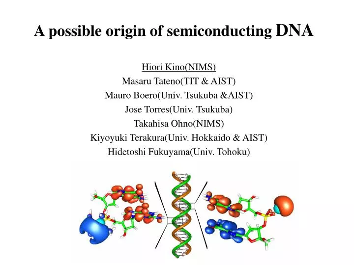
A possible origin of semiconducting DNA. Hiori Kino(NIMS) Masaru Tateno(TIT & AIST) Mauro Boero(Univ. Tsukuba &AIST) Jose Torres(Univ. Tsukuba) Takahisa Ohno(NIMS) Kiyoyuki Terakura(Univ. Hokkaido & AIST) Hidetoshi Fukuyama(Univ. Tohoku). Introduction DC conductivity measurements

E N D
A possible origin of semiconducting DNA Hiori Kino(NIMS) Masaru Tateno(TIT & AIST) Mauro Boero(Univ. Tsukuba &AIST) Jose Torres(Univ. Tsukuba) Takahisa Ohno(NIMS) Kiyoyuki Terakura(Univ. Hokkaido & AIST) Hidetoshi Fukuyama(Univ. Tohoku)
Introduction • DC conductivity measurements • Theoretical study so far • This work, theoretical study • Anderson localization
History • 1. Radiation damage • DNA is damaged by ultraviolet rays. • “How does a hole or electron created by ultraviolet rays move • in DNA?” • → electron transfer theory • 2. Is DNA metallic or insulating? • They measured DC conductivity.
Electron/hole hopping measurements in DNA UV energy LUMO (band) DNA in a living body Gap ~ 6-7eV UV light (trigger) m HOMO (band) If electrons/holes move rapidly, little radiation damage Motion of a existing hole/electron
I m ~T dry DNA mL mR (Landauer formula) If V is very small nF(w) Possibility of low energy excitation ~T Where does a hole/electron come from? ~Temperature w m V (trigger) DC transport measurement mR mL
energy LUMO (band) Gap ~ 6-7eV UV light (trigger) Chemical potential HOMO (band) Two kinds of exp. Electron transfer by UV light DC transport m ~T Energy scale < 102Kelvin Energy scale ~ 100eV No density of states→No transport Q. Finite DOS at m?
Etching technology of ultra-fine structures will encounter the barrier in the near future Nano device? • DNA : small crosssection (~2nm) • : self-assemble (utilizing complementary pairs of base molecules) Holliday junction Seeman’s cube Figures, from C. Dekker, Phys. World. 14, 29 (2001). • Low resistance useful nanowire
Another example 1.4kbase single-stranded DNA→octahedron Raw mages by cryo-electron microscopy Diameter~14nm W.M. Shih, et al., Nature, 427, 618 (2004).
DNA nano-machine DNA gear J. Am. Chem. Soc., 126 (37), 11410 -11411, 2004. “Molecular Gears: A Pair of DNA Circles Continuously Rolls against Each Other “ Ye Tian and Chengde Mao* DNA biped walking device Nano Letters, 4 (7), 1203 -1207, 2004 “A Precisely Controlled DNA Biped Walking Device “ (bike=二本足歩行) William B. Sherman and Nadrian C. Seeman*
Introduction • DC conductivity measurements • Theoretical study so far • This work, theoretical study • Anderson localization
l-DNA, scanning force microscopy ~105cm (>70nm) (T=RT) DC conductivity measurement Bundle of DNA De Pablo et al. Phys. Rev. Lett. 85, 4992 (2000)
l-DNA l-DNA 105Wcm (70nm) T=RT Summary of Experiments • Pablo et al. Phys. Rev. Lett. 85, 4992 (2000). l-DNA 106Wcm (4mm) T=RT? • Zhang et al. Phys. Rev. Lett. 89, 198102-1 (2002). 10-4Wcm(600nm-900nm),T=RT dG-dC Fink et al., Nature 398, 407(1999) 10-2Wcm (>20nm) dG-dC dG-dC 1Wcm (50nm) 10.4nm, T=100K-RT T=RT T=4.2K-RT Porath et al., Nature 403, 635(2000) Cai, et al., APL 77 (2000) 3105 Yoo, et al. RPL 87 (2001) 198102
insulator metal semiconductor E E E Metal,Insulator and doped semiconductor ~eV ~eV m m m schematically E E Band gap~T* m Conductivity of semiconductor several order of magnitude depending on the density of impurities Impurity host Thermally doped Intrinsically doped
Introduction • DC conductivity measurements • Theoretical study so far • This work, theoretical study • Anderson localization
base molecules backbone Structure of DNA G:C, A:T= hydrogen bond PO4= -1 charged, DNA=negatively charged system at pH~7 charge neutrality= cations (Na+, K+, Mg++,…) sugar PO4 Figures, from C. Dekker, Phys. World. 14, 29 (2001).
Theoretical Study Electronic structure of base molecules GpC: HOMO G LUMO C ApT: HOMO A LUMO T PW91/6-31G(d,p)
G C (acid) Poly(dG)-poly(dC) (PO4- is terminated by H+, the system is neutral) Theoretical study (2)Electronic structure of DNA C EF G e.g. HOMO band Blue=HOMO,Red=LUMO completely separated, G-C: hydrogen bonding Artacho et al. Mol. Phys. 101 (2003), 1587. DFT/GGA, SIESTA →Insulating(gap~2eV), (LDA underestimates band gap.)
Is semiconducting DNA possible? There can be some methods to dope carriers into insulating DNA. E.g. P is added to dope carriers into insulating Si. ppm order of P is sufficient to make Si conducting. E E ~eV Shift m ~eV m carriers! m insulator semiconductor
Introduction • DC conductivity measurements • Theoretical study so far • This work, theoretical study • Anderson localization
[(dG)2-X+?] (X:impurity) (With dopant) LUMO(C) hole m G impurity HOMO(G) G DOS(dopant) DOS(host) Intrinsic doping Poly(dG)-poly(dC) Possible electronic structures (Without dopant) LUMO(C) m HOMO(G) DOS
DNA in solution Condition of DNA in experiments C G H2O Dry DNA C G Most cation metals are with solvation shells, some may be anhydrous
Possible loci of cations(study of effects of solvation shell of catons) DNA cation There are many possible loci of cations. There may be many possible loci of cations which dope carriers into DNA. In this study, examine the electronic structure of one typical locus.
hydrated Mg anhydrous Mg cations cation (c) (c’) LUMO (GGA/PBE gap~0.7eV) LUMO@G LUMO (b) 7.6 eV (b) Mg+ HOMO Mg2+ Sz=0 Sz=1 SOMO (c’) (a) (a) Unoccupied state (b) B Occupied state (c’) (c) (b) (a) G G Calc. UHF/6-31G(d) [(dG)2Mg(H2O)n]+ PO4-1 Mg2+ Electronic structure of DNA hydrate v.s. anhydrous Mg C G
poly(dG)-poly(dC) with anhydrous Mg [(dG)2-Mg2+] Schematic electronic structure of dry DNA LUMO impurity m hole G HOMO m HOMO(G) DOS(dopant) DOS(host) • Intrinsic doping = localized spin moment at Mg # of injected holes into guanine HOMO band = # of anhydrous Mg
A. degree of drying Q. A possible origin of the diverse experimental results Maybe it is very hard to remove solvation shells. c.f. P@Si, ppm order Very small # of injected holes can make DNA conducting There will be a number of methods to dope carriers into insulating DNA chains. Experimental suggestion of another method of doping I3- , M. Taniguchi et al. Jpn. J. Apl. Phys. 42 (2003), L215 Comment: doping a hole is different from moving of the hole easily
C G structure cation Sz=0(para) Sz=0(AF) Sz=1(ferro) the most stable A Mg -2604.691 -2604.700 -2604.725 ferro B Mg -2604.680 -2604.711 -2604.711 AF/ferro A Zn -4182.521 -4182.581 -4182.555 AF B Zn -4182.482 -4182.546 -4182.536 AF A Ca -3081.868 -3081.864 -3081.838 para B Ca -3081.857 NG -3081.829 para Doping mechanism Other divalent cations Intrinsic Intrinsic Thermal? Unit: A.U., Gaussian 6-31G(d)/UHF abbreviation: A Mg = Mg@A-DNA PO4- X X PO4- J E E PO4- PO4- Mg+ Band gap~T* X PO4- PO4- X EF X PO4- PO4- X Mother material Impurity
Introduction • DC conductivity measurements • Theoretical study so far • This work, theoretical study • Anderson localization
If DNA has doped one-dimensional band → Anderson localization • In one-dimension, no mobility edge → the wavefunction is always localized. • Long-ranged hopping mechanism → maybe variable range hopping (VRH) Anderson localization E EF band Nonzero DOS at EF (Assumption of VRH=doped band) Polaron and so on. may be necessary at higher temperatures. We do not deny their theories. At very low temperature, Anderson localization plays important roles.
Stacked DNA into the gate I-V curve ---electronic contribution--- Log[ conductivity ] n=dimension+1 Mott VRH n=2 Efros-Shklovskii(ES) VRH Replot from Yoo, et al. RPL 87 (2001) 198102 n=2T0~90K (poly(dG)-poly(dC)) (103/T)1/2 (V) 4.2K a-1: localization length Non-ohmic conductivity OK! Nonohmic threshold band gap Exp. Yoo, et al. RPL 87 (2001) 198102. Theory. adopted the theory by H. Fukuyama and K. Yosida, J. Phys. Soc. Jpn. 46, 102 (1979).
Summary Anhydrous cation HOMO Hydrated cation SOMO J LUMO LUMO An injected hole • Intrinsic doping: Mg->ferro, Zn->antiferro • (Thermal doping: Ca ?) (Longer chains must be calculated ) # of anhydrous Mg or Zn, or thermally doped # of doped holes=
Comments The most stable structures of Mg@G2 Siesta (GGA+PCC): paramagnetic, HOMO=G, LUMO=Mg Gaussian98(HF): Ferromagnetic, SOMO=Mg, LUMO=G Guassian98(PW91PW91): Ferromagnetic, SOMO=Mg, LUMO=G In STATE(ultrasoft PS, GGA) and CPMD(GGA), to achieve self-consistency is harder. Ferromagnetic solution seems to be the most stable. Some LDA/GGA calculations of anhydrous Mg@DNA are unstable probably due to the self-interaction correction problem. Mg is spatially localized. Maybe it is connected with the result of siesta. Siesta uses localized PAOs which may raise the orbital energy of isolated Mg more than those of extended states of DNA base molecules. Careful consideration may be necessary to use PAOs in this case. (G: guanosine)
G O Mg++ P O- G Electronic structure of DNA (GGA/PBE) EF Paramag. (Sz=0) “Mg++” e(ev) G HOMO HOMO-1 HOMO LUMO siesta
Log[ conductivity ] (103/T)1/2 DNA exp. Doped semiconductors Replot from Yoo, et al. RPL 87 (2001) 198102 e ec textbook ed Log[nc] -1/2(ec-ed) Eg (ec-ed) -1/2 Eg 1/T DOS Aschcroft and Mermin, Solid State Physics, page 580 on ‘Homogenious Semiconductors’