Download
1 / 74
860 likes | 1.25k Views
Memory. Outline. Introduction RAM(DRAM&SRAM) ROM(EPROM, EEPROM, Flash) SOC(System-on-Chip) FRAM(Ferroelectric RAM) Summary. Memory. Memory can provide information (data) storage for future recalls Magnetic memory generally is capable of storing

E N D
Outline • Introduction • RAM(DRAM&SRAM) • ROM(EPROM, EEPROM, Flash) • SOC(System-on-Chip) • FRAM(Ferroelectric RAM) • Summary
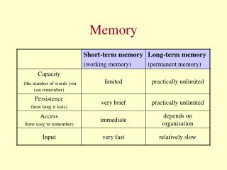
Memory • Memory can provide information (data) storage for future recalls Magnetic memorygenerally is capable of storing large amount of data at very low cost, but the access time (the time it takes to locate and then read or write) is usually very long • Semiconductor memoriesuse electrical signals to identify memory location and its information. The access time is much faster that magnetic memory
Semiconductor Memory Semiconductor memories are usually classified into two major types: volatile, or non-volatile. Volatile memories (SRAM, DRAM) loose their data once the power supply is turned off Non-volatile memories (ROM, EPROM) can retain their data even after power is removed
Candidates of Ideal Memory Memory attribute comparison High density DRAM EPROM Flash SRAM EEPROM Electrical Re-writability Nonvolatility
HDD HDD PCMCIA I/II Flash Memory Card ALU L1 L2 L3 CD RW CPU Chip DRAM DRAM DRAM DRAM DRAM DRAM DRAM DRAM DRAM DRAM DRAM DRAM DRAM DRAM DRAM DRAM DRAM DRAM Floppy Memories in PC Board Rack
Holographic memory HDD Capacity Optical Disc Flash SRAM MROM DRAM Speed Memories CPU L1 Cache Faster speed Second Level Cache (L2) Main Memory Hard Disk Drive
Conventional Memories Hard disk drive (HDD) Use magnetic bits Very low cost per MB Extremely slow High power consumption Shock prune Optical disc Use optical storage Low cost per MB All bad attributes of HDD
Semiconductor Memories Volatile Non-Volatile RAM ROM Mask ROM SRAM DRAM PROM 1970 by Intel 1970 by Intel 1970 by Intel EROM EEPROM 1971 by Intel Conventional FLASH 1984 by Toshiba 1979 by Intel
RAM • Random Access Memory (RAM) is a readable and write-able volatile memory • The term random access means that the user can access any location of the entire memory and in any order • RAM is further divided into dynamic RAM (DRAM) and static RAM (SRAM) • SRAM is a simple latch circuit (flip-flop) that remembers its state until it is toggled • DRAM is made of one switch and one storage cell
DRAM Cell Structure WORD LINE Column WORD LINE Row PASS TRANSISTOR CAPACITOR Transistor PLANAR PASS TRANSISTOR CAPACITOR Storage Capacitor WORD LINE CAPACITOR TRENCH PASS TRANSISTOR STACK
RAS CAS DRAM Architecture Memory Array address multiplexing word line delay Row Decoder Word-line Driver Row and Column Addresses Din Row Address Buffer Input Buffer Sense Amplifier I/O line Output Buffer Column Address Buffer Column Decoder Dout bandwidth Sense delay
Capacitor 3 2 4 PASS TRANSISTOR 1 Refresh • Junction leakage • Pass transistor subthreshold leakage • Leakage through capacitor dielectric • Other parasitic leakage paths
Scaling Trend • Minimum Feature Size : 0.7/Generation • Cell Area : 0.4 /Generation for Sensing and Soft-error Minimum Cell Capacitance: 25-30 fC • High-dielectric-constant material, BST, Ta2O5….. • Reduce dielectric film thickness • 3-D capacitor structure
Trench Cell >7 m Surface area is then large
Trench vs. Stacked • In the trench technology, the cell process is completed prior to the gate oxidation. Therefore, no thermal process coming from cell capacitor formation after the MOSFET fabrication is required. On the contrary, MOSFET formation is followed by cell capacitor in stacked structure • There is no height difference between cell array region and peripheral circuit region in the trench structure • In the stacked cell, the height difference demands high aspect ratio contact holes and then increases difficulty in the planarization process after the cell formation
Trench vs. Stacked • High temperature processing steps such as storage node insulator (SiO2/SiN) formation, SiN deposition for the self-aligned contact formation, etc. are commonly used in stacked cell • Salicide (Self Aligned siLICIDE) process for the source and drain of the MOSFETs should be carefully designed to endure the high temperature process steps • For applications requiring Embedded DRAM, trenched cell is more attractive because the DRAM cells are formed before the MOSFETs and because there is little height difference between the cell array and other regions on the chip
Applications Segments for DRAM • Computer • Main memory(PC, notebook,..) • Graphics subsystem, printers, fax • Consumer • Mobile systems, Video(TV, VCR) • Games • Communications • Switching system, Set top(ATM, MPEG2) • Industrial • Medical( X-ray video, scanners), Embedded processors
DRAM • Disadvantages • volatile • Somewhat lower speed • power consumption ( replenishing) • Advantages • high density • low cost DRAM still have the highest volume of memory market !!
SRAM VDD VDD VDD High Speed High Cost Low Density I WORD L H WORD VDD I-I I BIT BIT Six-transistor full CMOS
SRAM • Mainly used as Cache • SRAM are a quarter the capacity of DRAMs for the same process technology and chip size Cost about four times as much per bit as a DRAM!
ROM (Read Only Memory) • Mask ROM • Vedio Game • EPROM • Electrical Programmable • EEPROM • Electrically Erasable Programmable • Flash EPROM • Mainstream product
ROM (Read Only Memory) • As the name implies, read only memory has no provision to update or write its contents • The programming is usually done during manufacturing or by burning procedure prior to field use • ROMs can be considered as lookup tables where an address code input will produce a certain data at the output
ROM (Read Only Memory) • It can be programmed during manufacturing by photomask • Alternatively, it can be programmed by using fuse • This is called one-time-only programmable memory (OTP ROM) • Photomask is same for different contents • However, once it was programmed, its contents can not be changed
Floating Gate Charge-Trapping Control gate Poly-gate Floating gate ONO Blocking Oxide Si3N4 Tunnel oxide EPROM EEPROM Flash SONOS Types of NVM
- - - - - - - - Basic Operation Principle • Storage of charges Erased Programmed Gate QT Source Drain Darin Current Sense voltage n+ n+ P -sub Gate Voltage, VGS
Charge Transfer Mechanism • Hot-Electron Injection • Avalanche Injection • Channel Hot-Electron Injection • Source-Side Electron Injection • Substrate Injection • Fowler-Nordheim Tunneling • Ultraviolet Light Erase
What is “Hot Carrier”? • Carriers gain kinetic energy in the channel from electric field acceleration • For those carriers with higher energy than thermal energy (1/2kT) IEDM-99, Z.Chen
VG VD Channel Hot Electron Injection Gate and drain terminals are applied high voltage at the same time Pinch-off region control gate VS floating gate n+ n+ depletion region depletion edges
Fowler-Nordheim Tunneling Net bias is applied across gate oxide. For example, VG is high, S/D grounded VG B3.1eV Vox JQfT Si substrate SiO2 WKB approximation Gate Vox>B
UV erasing Control Gate I1 I2 Floating gate h1 Control Gate Source Drain h2 Substrate n+ n+ Floating Gate p-substrate EPROM(Electrically Programmable Read Only Memory)
EPROM(Electrically Programmable Read Only Memory) • Charges are stored in FG to alter the threshold voltage • Bit addressable • Not an in-system erasure; It should be removed from the board and placed under UV light for reprogramming its content. Usually, it takes 20 min. • Package is expensive since a quartz window is needed for UV light erasing • High density and low cost are its advantages
Inhibit Vpp GND Program Vpp W/L1 Inhibit Vpp W/L2 Forced Program B/L1 B/L2 Disturb in EPROM Vpp/2 GND Program Vpp Vpp/2 Forced Program B/L1 B/L2 Half Disturb Array Disturb
EPROM • Disturb issue makes EPROM can not be programmed by F-N tunneling (indeed, by CHE) • Same issue for erasure, therefore, UV light is needed • However, extremely long time required for UV light erasure andpackage is expensive • Over erasure could happen. Net positive charges in floating gate make devices operate in depletion state
Byte-Alterable Bit line Select- Line Word Line EEPROM(Electrically Erasable Programmable Read Only Memory) Control gate Floating gate Tunnel oxide Source n+ n+ p-substrate
Flash EEPROM Bit line ONO Word line n+ source n+ drain ph D G Programming : CHE, VG=12 V, VD =6.5V Erase: F-N tunneling, VS = 12 V, VG= GND, VD=floating VS = 5 V, VG= -10 V,VD=floating Array “Ground” S common source
Flash EEPROM • Density of EEPROM can not high since two transistors are needed • However, EPROM can not be erased electrically in system • High density, lost cost, high speed Flash EEPROM
Comparison of PROMs Source : Samsung
Bit by bit erase Bit line Select- Line Word Line What is Difference? EEPROM Flash EEPROM Block Erase Block 16KB, 64KB…
Applications Products & Capacity Tech-nology Mobile Comm. DECT, Pager, GSM (8、16M) NOR Computer PDA (8M), DCS (8M), BIOS (2~4M) NOR Multimedia DVD, MP3 (4M), DCS (8M), Storage card (above 16M) NAND AND Data Transfer S.T.B., Modem, Answering machine (4M) NAND AND Applications
Flash Memory Technologies Source : Samsung
Unit Cell Comparison Source : Samsung
Cell Architecture Source : Samsung
NOR Flash Source : Samsung