Download
1 / 53
560 likes | 1.08k Views
Chapter 3: Boolean Algebra and Digital Logic. CS140 Computer Organization. These slides are derived from those of Null & Lobur + the work of others. Chapter 3 Objectives. Understand the relationship between Boolean logic and digital computer circuits.

E N D
Chapter 3: Boolean Algebra and Digital Logic CS140 Computer Organization These slides are derived from those of Null & Lobur + the work of others. Chapter 3: Digital Logic
Chapter 3 Objectives • Understand the relationship between Boolean logic and digital computer circuits. • Learn how to design simple logic circuits. • Understand how digital circuits work together to form complex computer systems. Chapter 3: Digital Logic
3.1 Introduction • In the latter part of the nineteenth century, George Boole incensed philosophers and mathematicians alike when he suggested that logical thought could be represented through mathematical equations. • How dare anyone suggest that human thought could be encapsulated and manipulated like an algebraic formula? • Computers, as we know them today, are implementations of Boole’s Laws of Thought. • John Atanasoff and Claude Shannon were among the first to see this connection. • In the middle of the twentieth century, computers were commonly known as “thinking machines” and “electronic brains.” • Many people were fearful of them. • Nowadays, we rarely ponder the relationship between electronic digital computers and human logic. Computers are accepted as part of our lives. • Many people, however, are still fearful of them. Chapter 3: Digital Logic
3.2 Boolean Algebra • I’m assuming that you have taken or are currently taking Discrete Math. So I’m not planning on talking about Boolean algebra other than to connect it with circuits. • The Slides written by Null & Lobur have been moved to an Appendix at the end of this set. Chapter 3: Digital Logic
3.3 Logic Gates • Boolean functions are implemented in digital computer circuits called gates. • A gate is an electronic device that produces a result based on two or more input values. • In reality, gates consist of one to six transistors, but digital designers think of them as a single unit. • Integrated circuits contain collections of gates suited to a particular purpose. Vs – is ground = 0 Volts Vd – high voltage – for all the things we’re doing, this is +5V, but there are many possibilities. Vg – gate voltage – depending on this value, the electrons can or can not flow from high to low voltage. Chapter 3: Digital Logic
3.3 Logic Gates Voltage inverted from input Voltage from input This is the logic for an AND gate. It’s simply a NAND with an inverter. This is the logic for a NAND gate. Depending on the values of A, B, output C is connected either to Power or to Ground and so has either a 1 or 0 logical value. Chapter 3: Digital Logic
3.3 Logic Gates • The three simplest gates are the AND, OR, and NOT gates. • They correspond directly to their respective Boolean operations, as you can see by their truth tables. • And these representations map exactly into the transistors on the last two slides. 74LS08 Quad 2-input AND Chapter 3: Digital Logic
3.3 Logic Gates • The output of the XOR operation is true only when the values of the inputs differ. • Symbols for NAND and NOR, and truth tables are shown at the right. Note the special symbol for the XOR operation. 74LS02 Quad 2-input NOR Chapter 3: Digital Logic
3.3 Logic Gates • NAND and NOR are known as universal gates because they are inexpensive to manufacture and any Boolean function can be constructed using only NAND or only NOR gates. • Gates can have multiple inputs and more than one output. • A second output can be provided for the complement of the operation. • We’ll see more of this later. Chapter 3: Digital Logic
3.4 Digital Components • Combinations of gates implement Boolean functions. • The circuit below implements the function: • This is an example of a combinational logic circuit. • Combinational logic circuits produce a specified output (almost) at the instant when input values are applied. • Later we’ll explore circuits where this is not the case. Chapter 3: Digital Logic
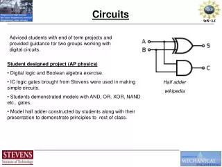
3.5 Combinational Circuits • Combinational logic circuits give us many useful devices. • One of the simplest is the half adder, which finds the sum of two bits. • We can gain some insight as to the construction of a half adder by looking at its truth table, shown at the right. • As we see, the sum can be found using the XOR operation and the carry using the AND operation. Chapter 3: Digital Logic
3.5 Combinational Circuits • We can change our half adder into to a full adder by including gates for processing the carry bit. • The truth table for a full adder is shown at the right. HALF ADDER FULL ADDER Chapter 3: Digital Logic
3.5 Combinational Circuits • Just as we combined half adders to make a full adder, full adders can connected in series. • The carry bit “ripples” from one adder to the next; hence, this configuration is called a ripple-carryadder. This is a 4-bit adder that you can program as part of your Project. 74LS283 Chapter 3: Digital Logic
3.5 Combinational Circuits • Decoders are another important type of combinational circuit. • Among other things, they are useful in selecting a memory location based on a binary value placed on the address lines of a memory bus. • Address decoders with n inputs can select any of 2n locations. • This is what a 2-to-4 decoder looks like on the inside. If x = 0 and y = 1, which output line is enabled? Chapter 3: Digital Logic
3.5 Combinational Circuits Chapter 3: Digital Logic
3.5 Combinational Circuits 74LS42 One of Ten Decoder Chapter 3: Digital Logic
3.5 Combinational Circuits • A multiplexer does just the opposite of a decoder. • It selects a single output from several inputs. • The particular input chosen for output is determined by the value of the multiplexer’s control lines. • To be able to select among n inputs, log2n control lines are needed. This is a block diagram for a multiplexer. Chapter 3: Digital Logic
3.5 Combinational Circuits • This is what a 4-to-1 multiplexer looks like on the inside. If S0 = 1 and S1 = 0, which input is transferred to the output? Chapter 3: Digital Logic
3.5 Combinational Circuits Chapter 3: Digital Logic
3.5 Combinational Circuits • This shifter moves the bits of a nibble one position to the left or right. If S = 0, in which direction do the input bits shift? Chapter 3: Digital Logic
3.5 Combinational Circuits 74LS164 8-bit shift register Chapter 3: Digital Logic
3.6 Sequential Circuits • Combinational logic circuits are perfect for situations when we require the immediate application of a Boolean function to a set of inputs. • There are other times, however, when we need a circuit to change its value with consideration to its current state as well as its inputs. • These circuits have to “remember” their current state. • Sequential logic circuits provide this functionality for us. • As the name implies, sequential logic circuits require a means by which events can be sequenced. • State changes are controlled by clocks. • A “clock” is a special circuit that sends electrical pulses through a circuit. • Clocks produce electrical waveforms such as the one shown below. Chapter 3: Digital Logic
3.6 Sequential Circuits State changes occur in sequential circuits only when the clock ticks (it’s “synchronous”) – otherwise the circuit is “asynchronous” and depends on wobbly input signals. Circuits that change state on the rising edge, or falling edge of the clock pulse are called edge-triggered. Level-triggered circuits change state when the clock voltage reaches its highest or lowest level. Chapter 3: Digital Logic
3.6 Sequential Circuits • To retain their state values, sequential circuits rely on feedback. • Feedback occurs when an output is looped back to the input. • A simple example of this concept is shown below. Yes, this little circuit shows feedback, but it never changes state: • If Q is 0 it will always be 0, if it is 1, it will always be 1. Why? • You can see how feedback works by examining the most basic sequential logic components, the SR flip-flop. • The “SR” stands for set/reset. • The internals of an SR flip-flop are shown, along with a block diagram. Chapter 3: Digital Logic
3.6 Sequential Circuits • The behavior of an SR flip-flop is described by a characteristic table. • Q(t) means the value of the output at time t. Q(t+1) is the value of Q after the next clock pulse. • The SR flip-flop actually has three inputs: S, R, and its current output, Q. (the Q is it’s state/history) • We can construct a truth table for this circuit, as shown at the right. • Notice the two undefined values. When both S and R are 1, the SR flip-flop is unstable. (meaning both Q and Q’ are 0 – and that’s not legal!) Try a set of inputs and see what you get on the outputs. Chapter 3: Digital Logic
3.6 Sequential Circuits • If we can be sure that the inputs to an SR flip-flop will never both be 1, we will never have an unstable circuit. This may not always be the case. So the JK flip-flop solves this problem. There’s no way for both S and R to both be 1, even if J and K are both 1. • At the right, is an SR flip-flop, modified to create a JK flip-flop. See how Q and Q’ condition the inputs to prevent S and R from both being 1. • The characteristic table indicates that the flip-flop is stable for all inputs. Means the value at t + 1 is the inverse of the value at t. Chapter 3: Digital Logic
3.6 Sequential Circuits 74LS112 Dual JK Negative Edge Flip Flop Triggers when the clock goes from high to low Chapter 3: Digital Logic
3.6 Sequential Circuits • Another modification of the SR flip-flop is the D flip-flop, shown below with its characteristic table. • The output of the flip-flop remains the same during subsequent clock pulses. The output changes only when the value of D changes. The previous state doesn’t matter. Totally dependent on state of D • The D flip-flop is the fundamental circuit of computer memory. • D flip-flops are usually illustrated using the block diagram shown here. Chapter 3: Digital Logic
3.6 Sequential Circuits 74LS174 Hex D Flip Flop Chapter 3: Digital Logic
3.6 Sequential Circuits • Sequential circuits are used anytime that we have a “stateful” application. • A stateful application is one where the next state of the machine depends on the current state of the machine and the input. • A stateful application requires both combinational and sequential logic. Chapter 3: Digital Logic
3.6 Sequential Circuits • This illustration shows a 4-bit register consisting of D flip-flops. You will usually see its block diagram (below) instead. A larger memory configuration is shown on the next slide. Chapter 3: Digital Logic
3.6 Sequential Circuits Chapter 3: Digital Logic
3.6 Sequential Circuits • A binary counter is another example of a sequential circuit. • The low-order bit is complemented at each clock pulse. • Whenever it changes from 0 to 1, the next bit is complemented, and so on through the other flip-flops. Chapter 3: Digital Logic
3.7 Designing Circuits • We have seen digital circuits from two points of view: digital analysis and digital synthesis. • Digital analysis explores the relationship between a circuits inputs and its outputs. • Digital synthesis creates logic diagrams using the values specified in a truth table. • Digital systems designers must also be mindful of the physical behaviors of circuits to include minute propagation delays that occur between the time when a circuit’s inputs are energized and when the output is accurate and stable. Chapter 3: Digital Logic
Computers are implementations of Boolean logic. Boolean functions are completely described by truth tables. Logic gates are small circuits that implement Boolean operators. The basic gates are AND, OR, and NOT. The XOR gate is very useful in parity checkers and adders. The “universal gates” are NOR, and NAND. Chapter 3 Conclusion Chapter 3: Digital Logic
Computer circuits consist of combinational logic circuits and sequential logic circuits. Combinational circuits produce outputs (almost) immediately when their inputs change. Sequential circuits require clocks to control their changes of state. The basic sequential circuit unit is the flip-flop: The behaviors of the SR, JK, and D flip-flops are the most important to know. The behavior of sequential circuits can be expressed using characteristic tables or through various finite state machines. Moore and Mealy machines are two finite state machines that model high-level circuit behavior. Chapter 3 Conclusion Chapter 3: Digital Logic
Appendix - 3.2 Boolean Algebra • Boolean algebra is a mathematical system for the manipulation of variables that can have one of two values. • In formal logic, these values are “true” and “false.” • In digital systems, these values are “on” and “off,” 1 and 0, or “high” and “low.” • Boolean expressions are created by performing operations on Boolean variables. • Common Boolean operators include AND, OR, and NOT. Chapter 3: Digital Logic
3.2 Boolean Algebra • A Boolean operator can be completely described using a truth table. • The truth table for the Boolean operators AND and OR are shown at the right. • The AND operator is also known as a Boolean product. The OR operator is the Boolean sum. Chapter 3: Digital Logic
3.2 Boolean Algebra • The truth table for the Boolean NOT operator is shown at the right. • The NOT operation is most often designated by an overbar. It is sometimes indicated by a prime mark ( ‘ ) or an “elbow” (). Chapter 3: Digital Logic
3.2 Boolean Algebra • A Boolean function has: • At least one Boolean variable, • At least one Boolean operator, and • At least one input from the set {0,1}. • It produces an output that is also a member of the set {0,1}. Now you know why the binary numbering system is so handy in digital systems. Chapter 3: Digital Logic
3.2 Boolean Algebra • The truth table for the Boolean function: is shown at the right. • To make evaluation of the Boolean function easier, the truth table contains extra (shaded) columns to hold evaluations of subparts of the function. Chapter 3: Digital Logic
3.2 Boolean Algebra • As with common arithmetic, Boolean operations have rules of precedence. • The NOT operator has highest priority, followed by AND and then OR. • This is how we chose the (shaded) function subparts in our table. Chapter 3: Digital Logic
3.2 Boolean Algebra • Digital computers contain circuits that implement Boolean functions. • The simpler that we can make a Boolean function, the smaller the circuit that will result. • Simpler circuits are cheaper to build, consume less power, and run faster than complex circuits. • With this in mind, we always want to reduce our Boolean functions to their simplest form. • There are a number of Boolean identities that help us to do this. Chapter 3: Digital Logic
3.2 Boolean Algebra • Most Boolean identities have an AND (product) form as well as an OR (sum) form. We give our identities using both forms. Our first group is rather intuitive: Chapter 3: Digital Logic
3.2 Boolean Algebra • Our second group of Boolean identities should be familiar to you from your study of algebra: Chapter 3: Digital Logic
3.2 Boolean Algebra • Our last group of Boolean identities are perhaps the most useful. • If you have studied set theory or formal logic, these laws are also familiar to you. Chapter 3: Digital Logic
3.2 Boolean Algebra • We can use Boolean identities to simplify the function: as follows: Chapter 3: Digital Logic
3.2 Boolean Algebra • Sometimes it is more economical to build a circuit using the complement of a function (and complementing its result) than it is to implement the function directly. • DeMorgan’s law provides an easy way of finding the complement of a Boolean function. • Recall DeMorgan’s law states: Chapter 3: Digital Logic
3.2 Boolean Algebra • DeMorgan’s law can be extended to any number of variables. • Replace each variable by its complement and change all ANDs to ORs and all ORs to ANDs. • Thus, we find the the complement of: is: Chapter 3: Digital Logic
3.2 Boolean Algebra • Through our exercises in simplifying Boolean expressions, we see that there are numerous ways of stating the same Boolean expression. • These “synonymous” forms are logically equivalent. • Logically equivalent expressions have identical truth tables. • In order to eliminate as much confusion as possible, designers express Boolean functions in standardized or canonical form. Chapter 3: Digital Logic