Download
1 / 20
200 likes | 338 Views
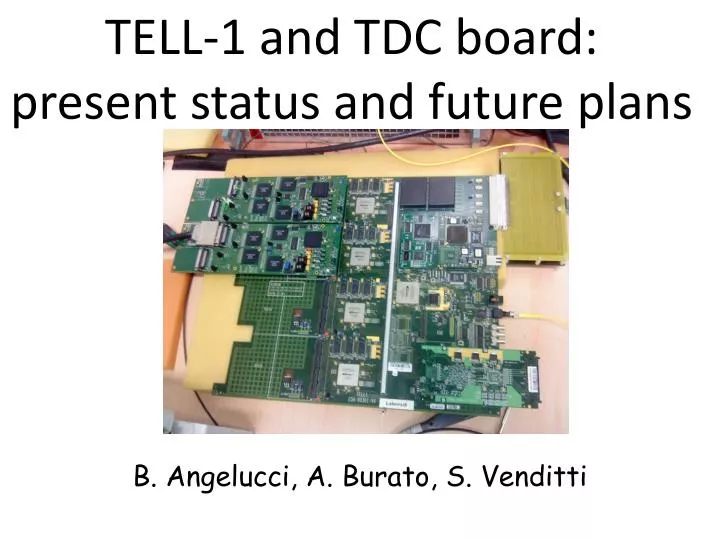
TELL-1 and TDC board : present status and future plans. B. Angelucci , A. Burato , S. Venditti. OUTLINE Improvements on hardware and firmware wrt previous reports Experimental setup used to perform tests Analysis of collected data Troubleshooting Where we stand and todo list.

E N D
TELL-1 and TDC board: present status and future plans B. Angelucci, A. Burato, S. Venditti
OUTLINE • Improvements on hardware and firmwarewrtpreviousreports • Experimentalsetupusedtoperformtests • Analysisofcollected data • Troubleshooting • Wherewe stand and todolist
NEW HARDWARE: TDCB • TDCB: V4 versiondelivered in Nov 2010: • New connectors, allowing the useofnewcables (standard SCSI). • Powersupplyplugmovedbymistakebyabout 2mm wrt the originalprojects, incompatiblewith TELL1/TEL62 TDCB V5 in production,first 2 expected in 2 weeks LVDS probe Cables Patch panel PG SCSI connectors
FIRMWARE: TDCB RAM PLL (clock 40Mhz) Transfer FIFO I2C Time Stamp Switch JTAG master TDC control QUARTUS II V.10.1
FIRMWARE: TDCB • TDCB can beprogrammedthrough a USB blastereitherdirectly (Active serial interface, .pof file) or indirectly (JTAG interface, .sof and .jicfiles) • The TDCB clock can betakendirectlyfrom FPGA’s PLL or refinedusing the TDCB internal QPLL • RAM blocksavailable (2 MB/TDCB), firmwareallowstowrite on thembutreadoutonlythrough I2C bynow JTAG chain
DATA FORMAT TDC data are in the formof 32 bit words leading 0x4 trailing 0x5 TDC TS TDC channel (32) Lead/trail #words in a TDC trigger 5 bit 4 bit 01010100010111010101100100010101 4 bit 19 bit eventtime (1 bit=98ps,TDC rollover =219=51,38µs) TDC number & board (4x4) TRIGGER MATCHING MODE Periodictriggers (12.8 µs normallyused) are sent to the TDCB in ordertoreadits data. Asearchwindow and a match windowmustbeproperly set tocollect the TDC words in the right time windows
THE GOAL • Setting up anautomated TDCB test system in viewof a massive TDCB production • Use ad hoc patternsto test some cryticalcharacteristicsof the TDCBs: resolution, sustainabilityof high rates, possiblefaultypaths on PCBs The presenttestswereperformed on only 8 channels and on the onlytwoavailable V4 boards, but up to 32 channels can bepresentlypulsed. The final test system willbeabletopulse 128/512 channels (1 TDCB/1 TELL62) at the sametime, usingpredeterminedpatterns
EXPERIMENTAL SETUP • The testsweperformed on the TELL1 and TDCBsrequire the followingitems: • A pattern generatorwithan input and output to trigger logicconditions in the pattern • A LTUvimoduletodistribute the trigger sequence (givenby the PG) to the TELL1 via the TTCexmodule • Probe(s) to produce LVDS signals (1 used in these tests+1 just bought, 16+16 LVDS signals) • NIM modulestoconvertdifferentlogicsignals (NIM, ECL,TTL) producedby the variousparts (PG, LTU) • At least 1 PCstobeusedbothas a server and tostore and analyze data (in oursetupweuse 2 differentPCsfor the twotasks) …andobviously a TELL1 with at least 1 TDCB!
Part of the pattern used (shiftedsignals) • 8 channelspulsedwith 20ns long pulses (min 10 ns) • PATTERN: • a) single channelspulsed, 12.8µs pause betweenpulses • b) allchannelspulsed at the sametime • c) single channelspulsed, 10 nsbetweenpulses(same TDCB TS) • useof input/output PG channelsto reset the TDCB TS at the beginningofeach pattern
LTU-PG-TELL1-PC COMMUNICATION Optical trigger to TELL1 Data to PC through GBE Trigin/out from/to PG to LTU module Signalconversions
LTU-PG-TELL1-PC COMMUNICATION • The PG sendsan output signal and waitsforan input • The output triggers the LTUvimodule, whichsends a reset signalto the TELL1 (causing TDC TS to reset) and a signal back to the PG input • After the input the PG sends 2 more signalsto the LTU through the output, which are sent as2 triggersto the TELL1. the 2 triggers are delayedtocollect the whole pattern. • The pattern isthencyclicallyrepeatedtill the acquisitionisstopped. ~ 0.2M pattern/min collected • Data are accumulated in the PP FIFOs and sent to the acquisition PC through a GBE connection when the TELL1 receives the LTUvi trigger (old TELL1 firmware)
DATA ANALYSIS The output from the TELL1 was sent through a GBE connection to the acquisition PC. Here data are turnedinto ROOT format in ordertobeeasilyanalyzed. Pulsedchannels: 4-7, 12-15 single signals (8 channels) 12,8 µs Allchannels (shifted) TS time Allchannels
Leadings and trailings in part b (channelspulsed at the sametime) and c (10 nsbetweenpulses) of the pattern CHANNELS 4,5,6,7,12,13,14,15
TRAILING-LEADING TIME CHANNELS 4,5,6,7,12,13,14,15
Pulsesfromallchannels (fired at the sametime at PG level) Offsetswillbeusedto eliminate channel-to-channelshifts
PROBLEMS DETECTED HOLES: oneTDC shows “holes” in the timedistribution TDC word timebins absolutetime (referredto first pulse)
GUESS: bit 0 and 1 paths are in contact, so that the output ofbits 0 and 1 isan OR oftheirrealsignals If so the truthtableshouldbe: TDC word timebins (detail) 2 emptybinsevery 4, 1/3 ratiobetween the other 2 and that’s it!
NOISY CHANNELS A long timeproblem on noisychannels (seeMarco’s last meeting presentation) wasunderstood, the cause beingthat the channelsnotpulsedwerenotproperlyterminated. Thiscaused a noisealmost in timewith the signal, whichlookedlike cross talk. A new patch panel (input PG, output TDCB cable), alreadyavailable, will solve thisproblem. 16 unterminatedchannels 16 pulsedchannels Pulsedchannels: 4-7, 12-15
Conclusions • A (very) preliminary procedure to test TDC boardshasbeen set up • No data loss detected at the levelof the collectedstatistics (~107events) • Resolutioncompatiblewith 100ps (~1 TDC bit), PG effectstilltobeunderstood (probablysizeable) • Some problemshavebeendetected, some ofthemweresolved, many more willcome… Todolist • Produce a TDCB test programanalyzing data and comparingthemwith the PG pattern • High rate tests • Offset adjustmentof TDC channels • Trytochange trigger windows • Firmwaredevelopment