Download
1 / 40
410 likes | 499 Views
SPIROC READOUT FOR PEBS. W. Karpinski I. Physikalisches Institut. Geneva, 28 January 2009. Outline. SPIROC global overview Description of the Readout Board for 128 channels First measurements Summary. SPIROC main characteristics. SPIROC : Silicon Photomul .

E N D
SPIROC READOUT FOR PEBS W. Karpinski I. Physikalisches Institut Geneva, 28 January 2009 Waclaw Karpinski
Outline • SPIROC global overview • Description of the Readout Board for 128 channels • First measurements • Summary Waclaw Karpinski
SPIROC main characteristics • SPIROC : SiliconPhotomul. IntegratedReadout Chip • 36 channels • two gains (1:10) • positive input pulse • DAC on each input • Charge measurementfrom 1pe to 2000 pe(atSiPm gain 1 x 10⁶ el) • Time measurementwith the accuracy of 100 ps • Autotrigger on 1/3 pe • complex digital part to transfer the data to DAQ • Chips daisy-chained • Chip size: 4.2mm x 7.2mm • Package QFP-240 • 0.35µm SiGetechnologyfrom AMS Waclaw Karpinski
0.1pF-1.5pF 1.5pF Slow Shaper Analog memory 25 -175ns Low gain Preamplifier Gain Gain selection Depth 16 Slow Shaper 12-bit Wilkinson ADC 0.1pF-1.5pF Charge measurement 15pF 25-175ns Depth 16 READ HOLD IN High gain Preamplifier Fast Shaper Conversion 100 µs Variable delay 10ns Discri Trigger Flag TDC 8-bit DAC 0-4.5V Depth 16 4-bit threshold adjustment DAC output Time measurement TDC ramp 300ns/5 µs 10-bit DAC Common to the 36 channels SPIROC : One channelschematic IN test Waclaw Karpinski
ValidHoldAnalogb gain gain Wilkinson ADC Discri output Wilkinson ADC Discri output Trigger discri Output Trigger discri Output Conversion ADC + WritingRAM RAM 16 RazRangN Chipsat 16 ReadMesureb 16 Acquisition NoTrig ExtSigmaTM (OR36) StartAcqt SlowClock Hit channel register 16 x 36 x 1 bits TM (Discri trigger) BCID 16 x 8 bits 36 Channel 0 StartConvDAQb 36 ValGain (low gain or high Gain) TransmitOn readout RamFull OutSerie 36 EndReadOut EndRamp (Discri ADC Wilkinson) StartReadOut Rstb FlagTDC Channel 1 Clk40MHz ..… ADC ramp Startrampb (wilkinson ramp) OR36 … StartRampTDC TDC ramp ChipID Chip ID register 8 bits 8 ASIC ValDimGray DAQ ValDimGray 12 bits 12 Waclaw Karpinski
Chip for SiPM : SPIROC three 36*16 Analog memories 36 Preamp Shaper discri 36 Wilkinson ADC 36 8bit 5V DAC SRAM Readout Bandgap Dual DAC Waclaw Karpinski
Time betweentwobunchcrossing: 337 ns Time between two trains: 200ms (5 Hz) time Train length 2820 bunch X (950 µs) A/D conv. DAQ IDLE MODE Acquisition 1ms (.5%) .5ms (.25%) .5ms (.25%) 198ms (99%) 99% idle cycle 1% duty cycle ILC beam structure • two orders of magnitude saved on the power consumption • the anticipated power consumption 25 µW/channel Waclaw Karpinski
Pulse at analog output as a function of shaping time injected charge =18.7 x 10⁶ el. , High-Gain, CFB=100 fF SPIROC in CQFP-240 25ns 50ns 75ns 125ns 175ns Preset Value vs Measured Value 25 ns 55 ns 50 ns 75 ns 75 ns 95 ns 100 ns 110 ns 125 ns 125 ns 150 ns 140 ns 175 ns 150 ns Test board designed by Orsay group Waclaw Karpinski
Pulse Amplitude on SPIROC Output • Two gain ranges: High and Low • In each range gain adjustable • with feedback capacitors • 4 bits resolution: • Cfb = 0.1fF, 02fF, 04fF,0.8fF • dynamic range in the high gain: • from spe to 200 pe (atSiPm gain 1 x 10⁶ el) HIGH GAIN [mV] LOW GAIN • in low gain range • energy measurement • up to ~2000 pe Waclaw Karpinski
Single photoelectronspectrum SPIROC & Hamamatsu SiPmS10362-11-100C (gain ~2x10⁶) Vbias =70.2 V, I=0,60 µA Shaping Time = 25 ns (presetvalue) High Gain Feedback Cap. = 100 fF S/N = 7.7 +/- 0.2 Waclaw Karpinski
Single photoelectronspectrum SPIROC & Hamamatsu SiPmS10362-11-100C (gain ~2x10⁶) Vbias =70.2 V, I=0,60 µA Shaping Time = 25 ns (setvalue ) High Gain Feedback Cap. = 200 fF Waclaw Karpinski
Single photoelectronspectrum SPIROC & Hamamatsu SiPmS10362-11-100C (gain ~2x10⁶) Vbias =70.2 V, I=0,60 µA Shaping Time = 75 ns (presetvalue) High Gain Feedback Cap. = 100 fF S/N = 6.6 +/- 0.2 Waclaw Karpinski
Single photoelectronspectrum SPIROC & Hamamatsu SiPmS10362-11-100C (gain ~2x10⁶) Vbias =70.2 V, I=0,60 µA Shaping Time = 100 ns (presetvalue) High Gain Feedback Cap. = 100 fF S/N = 5.4 +/- 0.3 Waclaw Karpinski
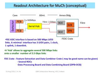
Readoutboard HPE_SPIROC-128 • analog, multipexed readout of 128 channels • 4 Spiroc chips, 32 channels per chip • chips mounted on a pluggable chip • carrier • interface to the DAQ compatible with TDR • download of slow control • parameters via USB or SPI interface SPIROC 16 mm SPI Interface 13 mm Interface to TDR USB Interface Waclaw Karpinski
Functionality of the CPLD • SPIROCs slow control register consist of 702 bits. • The data for up to 8 SPIROCS stored in the UFM block of the • AlteraMAXII CPLD • The data stored in the UFM Block can be modified from higher DAQ • using SPI or USB Interface. • After power up the data will be automatically downloaded from CPLD • to the SPIROC • After downloading the state machine automatically compares the data • stored in the CPLD and in the SPIROC chips, simultaneously • counts the number of errors and stores the result in 8 registers and • 8 error flags • For simplicity LED are implemented to indicate the status of the error • flags • CPLD decodes also the control signals sent from TDR • allows channel selection without higher DAQ . The channel number is • transferred via SPI or USB Interface Waclaw Karpinski
Graphical Interface to modify Control Parameters Waclaw Karpinski
First Result • the readout board operational • 12 chips assembled on the chip carriers • yield of the chips ~50% • if register outputs not used yield ~ 85% analog outputs broken during commissioning because of bag in the bonding program Waclaw Karpinski
Slow control register • Problem with the length of slow control register: • inside the chip, there are 703 flip-flops • on the test board form Orsay the tests show that one flip-flop • is missing, only 702 bits programmable • on our tests boards we see only 701bits • The behavior is stable and the same for all measured chips • due to the chip designer the reason are some fan-out issues • on the data and the clock paths of the slow control register. • . Waclaw Karpinski
Analog Output • for small signals standard deviation of base line and signal peak the same • for large signals standard deviation of signal peak significantly higher than • of the base line • this behavior is not observed on test board from Orsay Test pulse response; High gain, Cfb=100fF, shaping time 25 ns sdev=8.4mV sdev=3.3mV sdev=3.3mV sdev=3.9mV Waclaw Karpinski
Analog Output • high gain, Cfb=100fF, T=25ns • for small signals: spe/noise= 10 • for large signals: spe/noise= 2 • Gain uniformity: RMS 1% • all tested chips show similar behavior Waclaw Karpinski
Single photoelectron spectrum Aachen readout board • Spectra taken with both readout boards: Aachen and Orsay under the same conditions: • High gain, Cfb=100fF, T=25ns • Hamamatsu SiPm S10362-11-100C • Vbias =70.2 V, I=0,60 µA • no significant differences in gain and noise • performance between the readout boards Orsay readout board Waclaw Karpinski
Analog Output • low gain, Cfb=1.5pF, T=25ns • noise independent of the signal amplitude • gain uniformity: RMS 7% Waclaw Karpinski
Multiplexed Readout Pedestal uniformity: Avg = 789 mV RMS = 11.4 mV equal noise of all channels Waclaw Karpinski
INPUT DAC 36 DACs, one per channel 8 bit, 2.5V range LSB ~10mV very low power consumption ~1µW can absorb up to 10 µA leakage current from SiPm linearity: ± 2% Waclaw Karpinski
PowerConsumption • Total Power Consumption ~ 390 mW/chip →10.8mW/ch • Breakdown of the power consumption: • preamplifier+shaper = 4 mW/channel • SCA = 5.6 mW/channel • auxiliary parts (not consciously used) =2.2 mW/channel • Not acceptable for Tracker ! • Investigation of possibilities leading to significant reduction of power consumption necessary • backup solution: VA32-75 or its successesor Waclaw Karpinski
AnalogOutputImpedance • SPIROC has not a high impedance analog output • the analog outputs can not be connected in daisy chain • directly • one possibility is to implement an analog multiplexer • between the SPIROC outputs Waclaw Karpinski
SPIROC-Summary Waclaw Karpinski
Summary • charge measurement from 1 pe to 2000 pe (at SiPm gain of 1 x 10⁶ ) in two • linear scales • S/N of 10 w/o noise contribution from the detector, • however on Aachen readout board additional jitter of the • signal peak observed for input signals larger than 15 pe (at highest gain) • good pedestal and gain uniformity between channels on one chip • Ultra low power, 8bit input DAC for SiPM gain adjustment on each • channel, resolution and range adjustable. • on Aachen readout board the resolution=10 mV, range=2.5 V • yield of the chip production low ~50%, (~ 85% ) • high power consumption 10,8 mW/channel ! • to much for PEBS Fiber Tracker • investigation of options leading to significant reduction of the power • consumption necessary Waclaw Karpinski
Backup Transparences Waclaw Karpinski
SPIROC main features • Internal input 8-bit DAC (0-5V) for individual SiPM gain adjustment • Energy measurement : 14 bits • 2 gains (1-10) + 12 bit ADC 1 pe 2000 pe (300pC) • Variable shaping time from 25ns to 175ns • pe/noise ratio : 10 • Auto-trigger on 1/3 pe (50fC) • pe/noise ratio on trigger channel : 24 • Fast shaper : ~10ns • Time measurement : • 12-bit Bunch Crossing ID • 12 bit TDC step~100 ps • Analog memory for time and charge measurement : depth = 16 • Individually addressable calibration injection capacitance • Embedded bandgap for voltage references • Embedded 10 bit DAC for trigger threshold and gain selection • Multiplexed analog output • 4k internal memory and Daisy chain readout Waclaw Karpinski
Input preamp • Bi-gain low noise preamp • Low noise charge preamp • capacitively coupled = voltage preamp • High gain - 15 pF coupling capacitor • Low gain - 1.5pF coupling capacitor • MAX : 2000 pe ( at SiPm gain 1 x 10⁶) =300pC • Gain adjustable with 4 bits common to • all preamps : Cf=0.1, 0.2, 0.4, 0.8 pF • Positive input pulse • Power specified: 2 mW (unpulsed) • measured: 4 mW 0.1pF-1.5pF 15pF +HV 8-bit DAC Si PM High voltage on the cable shielding ASIC Waclaw Karpinski
VA75-32 Chip 32 cell bit-register 32 cell bit-register 32 x Analogue Mux. 32 cell bit-register 32 x Analogue Mux. Waclaw Karpinski
VA32-75 Chip -Summary Waclaw Karpinski
VA duringbeam test S/N=6.08 Waclaw Karpinski
HARDROC HARDROC has been designed to read out the CALICE RPC DHCAL technical prototype. Waclaw Karpinski
HARDROC main features • Full power pulsing • Digital memory: Data saved during bunch train. • Only one serial output @ 1 or 5MHz • Store all channels and BCID for every hit. Depth = 128 bits • Data format : 128(depth)*[2bit*64ch+24bit(BCID)+8bit(Header)] = 20kbits • BASICALLY : MAROC with internal RAM and time counting Waclaw Karpinski
HARDROC Summary Waclaw Karpinski
Slow shaper & SCA • Slow shaper from HaRDROC • Variable peaking time • 3 bits common to all channels • specified : 25-175 ns • Backup : analog S&H • Hold capacitor : 0.5 pF • Needs external hold signal • Multiplexed analog output @ 5MHz • SCA • = multiple S&H • Depth = 16 • Droop < 1 mV/ms • Hold signal generated internally with adjustable delay Slow Shaper Analog memory Depth 16 Waclaw Karpinski
Time between two bunch crossing: 337 ns Time between two trains: 200ms (5 Hz) time Train length 2820 bunch X (950 µs) A/D conv. DAQ IDLE MODE Acquisition 1ms (.5%) .5ms (.25%) .5ms (.25%) 199ms (99%) 99% idle cycle 1% duty cycle A/D conversion Acquisition DAQ • The data (charge) stored in the analogue memory are sequentially converted in digital and stored in a SRAM. • An event in RAM is : • The Bunch Crossing ID • The charge • The shaper gain • The status of the trigger The eventsstored in the RAM are outputtedthrough a serial linkwhen the chip gets the tokenallowing the data transmission. When the transmission isdone, the tokenistransferred to the next chip. 256 chips canberead out through one serial link • When an event occurs : • Charge isstored in analogue memory • Time isstored in digital (Bunchcrossing ID) memory • Trigger isautomaticallyrearmedatnextbunchcrossing ID • Depht of memoryis 16 ILC beam structure Two orders of magnitude saved on the power consumption Waclaw Karpinski
Read out : token ring 1 event 5 events 3 events 0 event 0 event Chip 0 Chip 1 Chip 2 Chip 3 Chip 4 Data bus Chip 0 A/D conv. DAQ IDLE MODE Acquisition Chip 1 A/D conv. IDLE DAQ IDLE MODE Acquisition Chip 2 A/D conv. IDLE IDLE MODE Acquisition Chip 3 A/D conv. IDLE IDLE MODE Acquisition Chip 4 A/D conv. IDLE DAQ IDLE MODE Acquisition Waclaw Karpinski