Download
1 / 27
270 likes | 433 Views
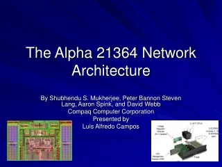
Alpha 21364. Goal: very fast multiprocessor systems, highly scalable Main trick is high-bandwidth, low-latency data access. How to do it, how to do it?. Fast access to L2 cache. Easy solution: put it on chip Technology scaling has made it practical.

E N D
Alpha 21364 • Goal: very fast multiprocessor systems, highly scalable • Main trick is high-bandwidth, low-latency data access. • How to do it, how to do it?
Fast access to L2 cache • Easy solution: put it on chip • Technology scaling has made it practical. • Higher bandwidth, lower latency, but smaller size than SRAM. • Many design and CAD problems.
Fast access to main memory • Build a NUMA system. • Each CPU directly controls its main memory chips (no intervening chipset). • On-chip RAMBus memory controller • Multiple frequencies cause design and CAD problems.
Fast remote memory access • Direct communication with other CPUs. • 2-D torus (folded checkerboard) • Switchbox/router on chip for passing packets between any 2 grid points. • Clock-forwarded data via matched T-lines. • Many design and CAD challenges.
All of that, and FAST • Greater than 1 Ghz in initial part. • Faster shrinks to follow. • Many design and CAD challenges!
One-chip scalable system Mem CPU CPU Mem Mem CPU CPU Mem
It gets worse • Much of this has been designed before -- by trial and error. • Now it’s part of a full-custom CPU. • Must be right the first time.
L2 cache • We are combining memory and logic in a high-speed part. • Cache covers a large die area, but is synchronous and needs a clock. • Many conditional clocks are needed to save power. • Problem: how do we control/simulate clock skew?
H tree? • H tree has nominal 0 skew at terminuses. • Real life must include OCV: • L, , sheet , C • Vdd, T • How do we minimize the sensitivity of skew to OCV?
L2 cache logic verification • A cache is not a simple animal. • The “simple” high-level picture is complicated by redundancy, BIST/BISR, fuse farms, optimal repair algorithms, complex circuit design. • Needs verification of RTL and schematics
Too big to verify? • Flat? 4 MB virtual memory / 100M Mos = 40 B/MOS. • The cache is “not quite” hierarchical. • ECC gets in the way (odd # of bits) • mirrored bank pairs share logic • The “same” path may be a race or a critical path in different banks.
Formal verification? • Symbolic simulation of something this big (e.g., with STE) is impossible. • Redundancy is an interesting challenge. • We can verify the pieces: but how do we prove they equal the whole?
The abstraction gap • The model must run fast • The schematics contain 100M devices. • Thus there is an abstraction gap. • This makes formal verification difficult.
Fast access to main memory • Build a NUMA system. • Each CPU directly controls its main memory chips (no intervening chipset). • On-chip RAMBus memory controller • Multiple frequencies cause design and CAD problems.
On-chip Rambus Controller • 400 Mhz dual data rate Rambus • > 1 Ghz CPU • How do they interact?
Fast remote memory access • Direct communication with other CPUs. • 2-D torus (folded checkerboard) • Switchbox/router on chip for passing packets between any 2 grid points. • Clock-forwarded data via matched T-lines. • Many design and CAD challenges.
On Chip Switchbox/router • Message passing usually handled by chipsets. • Now it’s on the CPU • We’ve got to get it right the 1st time.
Routers are tricky • Deadlock, Livelock • Route around broken links • Easy to forget corner cases • Formal verification is a must
High speed CPU • Clocking is a challenge. • Short tick is a challenge. • OCV is a killer. • Power density is also.
Clocking • Wires do not scale (even with copper). • Low clock skew = high clock power. • No longer practical to have a single main clock grid.
Multiple grids • Solution - multiple grids linked by Delay Locked Loops (DLLs). • Use skew-insensitive circuits to cross clock domains. These are functional at any skew (albeit with slower clock frequency). • How do you do static timing verification?
Short tick • “Short tick” CPU is highly pipelined, with small amount of gates between latches. • Most of the design is single-wire clocking, true single phase. • Races are bad.
Double-sided constraints • Tdmax + Tsetup < Tcycle + Ts,min • Tdmin > Thold + Ts,max • Short tick and large delay variation give you a small design window.
OCV • OCV gets worse every generation. • Higher density more T, more V. • Smaller feature size more variability. • Result is more delay variation.
Statistical delay correlation • Many delays are correlated. • Most “nearby” effects move together. • If two clocks have identical layout, they mostly move together. • Howe do we quantify this and use it in timing verification?
Summary • Alpha 21364 is a high-speed CPU targeted at glueless, scalable MP systems. • On-chip L2 cache • On-chip Rambus controllers • On-chip Routing • Many new CAD challenges - not all have solutions identified.