Download
1 / 16
160 likes | 242 Views
Development of a High Density Pixel Multichip Module at Fermilab. S. Zimmermann, G. Cardoso, J. Andresen, J.A. Appel, G. Chiodini, D.C. Christian, B.K. Hall, J. Hoff, S.W. Kwan, A. Mekkaoui, R. Yarema Fermi National Accelerator Laboratory Batavia, IL 60510 USA zimmer@fnal.gov.

E N D
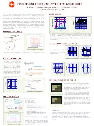
Development of a High Density Pixel Multichip Module at Fermilab S. Zimmermann, G. Cardoso, J. Andresen, J.A. Appel, G. Chiodini, D.C. Christian, B.K. Hall, J. Hoff, S.W. Kwan, A. Mekkaoui, R. Yarema Fermi National Accelerator Laboratory Batavia, IL 60510 USA zimmer@fnal.gov Work supported by the U.S. Department of Energy under contract No. DE-AC02-76CH03000. Fermilab Conf-01/247-E LEB 2001September 11th, 2001
Outline • Introduction • Proposed Pixel Detector MCM • Baseline Design • Constraint: data rate • Characteristics of the flex circuit technology • Pixel MCM Prototype • PCI test stand • Experimental results • Conclusions Development of a High Density Pixel Multichip Module at Fermilab
Introduction :BTeV Pixel Detector • Pixel half plane: approximately 510 cm2. • 868 pixel modules • Position: 6 mm from the beam. • “Shingle” approach allows for 100% coverage in a single plane side. Development of a High Density Pixel Multichip Module at Fermilab
Pixel Multichip Module – Baseline Design Point-to-point Connection Development of a High Density Pixel Multichip Module at Fermilab
Constraint: Data Rate • The Pixel detector will be used for the lowest level trigger all pixel hit data needs to be readout • Simulation: assume • Luminosity of 21032 cm2s1 ( an average of two interactions per crossing) • Threshold: 2000 e– • Magnetic field: 1.6 T • Does not use the angle required for “shingling” • Chip data rate depends on: • Chip active area • Distance from the beam • Number of pulse height ADC bits; assume 3 bits • The way the data is arranged, etc. Development of a High Density Pixel Multichip Module at Fermilab
Example: Column with more hits Beam Chip with more hits Development of a High Density Pixel Multichip Module at Fermilab
Experimental Layout for FPIX2: • Fine-pitch traces and spacing - 50m • Multilayer: presently 4 layers, goal 3 layers • Small via cover pads - 200m • Problems with outgassing and ferromagnetism • Small production quantities (by industry standards) Development of a High Density Pixel Multichip Module at Fermilab
Digital lines Analog lines Metal Layer 1 Layer 1 Metal Layer 2 Digital Analog Flex Circuit Metal Layer 3 Layer 2 Ground High Voltage Metal Layer 4 Layer 3 2 Bias Pad (1mm ) Adhesive Gold Epoxy Bias Window Silicon Sensor 4 Layer Flex Circuit Cross Section Development of a High Density Pixel Multichip Module at Fermilab
Pixel Multichip Module Prototype • Uses FPIX1 • Two modules characterized: • Single chip bump bonded to single SINTEF sensor (Indium) • Single chip without sensor • Flex circuit laminated onto sensor • Up to 5 Readout chips wire-bonded to flex circuit • Closer to final module Development of a High Density Pixel Multichip Module at Fermilab
Dimensions: 98.5mm x 10.25mm • Line width: 35m • Line to line clearance: 35m • Metal layer thickness: 10m • Number of layers: 4 • Via pad: 108m • Lamination: 5m epoxy • Film thickness (Apical): 25m Flex Circuit made by CERN Top Connectors Wire bonding pads Decoupling Caps. Bottom Terminations H.V. Development of a High Density Pixel Multichip Module at Fermilab
Single chip (FPIX1) without sensor LVDS drivers Connectors to DAQ Wire bonds Readout IC Flex Circuit Development of a High Density Pixel Multichip Module at Fermilab
Single chip (FPIX1) with SINTEF sensor (Indium bumps) LVDS drivers Connectors to DAQ Wire bonds Flex Circuit Readout IC Sensor Development of a High Density Pixel Multichip Module at Fermilab
PCI Test Stand • FPGA controlling all functions • PCI interface • 4MB of RAM • Daughter card interface (IEEE1386) • JTAG • USB • RS232 Pixel Module Development of a High Density Pixel Multichip Module at Fermilab
Characterization Results [e-] Development of a High Density Pixel Multichip Module at Fermilab
Pixel Module with Sensor Hit Map (Sr90) Development of a High Density Pixel Multichip Module at Fermilab
Conclusions: • Good agreement between circuit simulation and real measurements • Good performance characteristics. • No significant increase in noise and threshold dispersion when compared with previous single chip prototypes • No crosstalk problems between the digital and analog sections of the readout chip and flex circuit. Development of a High Density Pixel Multichip Module at Fermilab