Download
1 / 9
90 likes | 256 Views
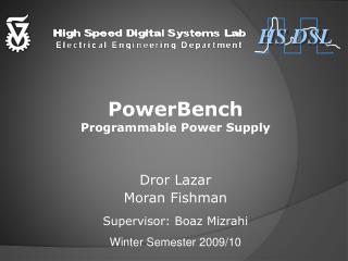
HS DSL. PowerBench Programmable Power Supply. Dror Lazar Moran Fishman Supervisor: Boaz Mizrahi Winter Semester 2009/10. Project Overview - Reminder. A versatile power supply unit with multiple outputs for laboratory use and testing of various electronic devices.

E N D
HS DSL PowerBench Programmable Power Supply Dror Lazar Moran Fishman Supervisor: Boaz Mizrahi Winter Semester 2009/10
Project Overview - Reminder A versatile power supply unit with multiple outputs for laboratory use and testing of various electronic devices.
OverviewA brief reminder Overview A brief reminder User interface D U T Power supply Control unit Measurement unit Active load User interface for standalone operation LEDs LCD Keys
OverviewControl Scheme Overview Control Scheme DAC Output setting DC-DC Converter Post regulator Current Sense Controller Block & Registers Input voltage sense feed- forward PWM Output AuxiliaryVoltage Sense ADC Tempe-rature Current limit ADC Voltage Sense ADC Microprocessor FPGA
Implementation 1) System & Board design (2 semesters)– completed 3 separate boards : - “Digital” – control board - “Analog” – sink/source/measurement (SSM) - “Panel” – user interface (UI) 2) Hardware bring-up & FPGA design (semester) – our project - Analog board bring-up, Digital board power-path debug - FPGA design : A/D & D/A interfaces, PWM, SMPS controllers - PC –> Cypress –> PIC basic implementation - PIC – FPGA interface 3) Software design (semester) – another project - PIC microprocessor software - Cypress USB controller software - PC drivers and applications
Analog Board Bring-Up • - Buck converters • Buck converters A/Ds • LDOs • LDOs D/As • LDOs A/Ds • Cuk converter • Cuk converter A/D • Source operation : • - Full-path bring-up : PC USB PIC FPGA Bucks / Cuk LDOs • DUT • - PWM duty-cycle step response with various loads connected to LDOs • outputs • Load operation : • - FPGA configures path to load mode. • - FPGA configures load-circuit D/A to constant current sink. • - connecting laboratory power supply, checking current sink. • - changing current sink amount – checking step response.
FPGA Controller Design PC – PIC – FPGA Interface Design 2 control loops : Bucks / Cuk control loop LDOs control loop implement controller using SMPS controller design principles. integrate with A/D & D/A interfaces in FPGA check controller performance : step response, O.S, settling time • designing communication protocol to PIC microprocessor using SPI interface (registers in FPGA) • implementing basic software in PC & PIC – different scenarios in Source & Load modes. • check FPGA measurements from A/Ds in both modes with PC software
Timetable System introduction Verilog learning FPGA configuration- LDOs,2-ch A/D,D/A Bring up Negative channel Bring up (Cuk) Design FPGA Modules req. for Bucks bring-up SMPS controller Design – 2 loops Mid semester Presentation FPGA modules simulations Full path debug – Source operation FPGA configuration- Bucks,4-ch A/D Bring up Full path debug – Load operation Design FPGA Modules for LDOs bring-up Final Presentation Char. Presentation Digital board Power path debug PIC – FPGA Interface design