Download
1 / 2
20 likes | 90 Views
Uniform Coating of Convoluted Structures by Static CVD John R. Abelson, University of Illinois at Urbana-Champaign, DMR 1005715.

E N D
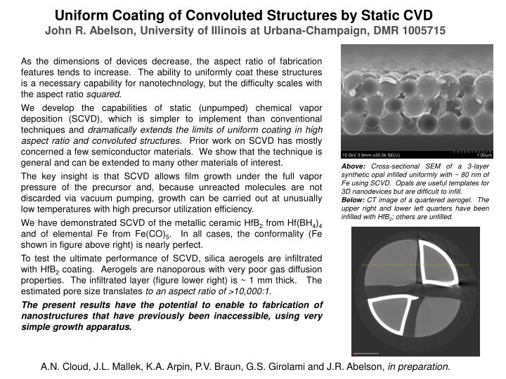
Uniform Coating of Convoluted Structures by Static CVDJohn R. Abelson, University of Illinois at Urbana-Champaign, DMR 1005715 As the dimensions of devices decrease, the aspect ratio of fabrication features tends to increase. The ability to uniformly coat these structures is a necessary capability for nanotechnology, but the difficulty scales with the aspect ratio squared. We develop the capabilities of static (unpumped) chemical vapor deposition (SCVD), which is simpler to implement than conventional techniques and dramatically extends the limits of uniform coating in high aspect ratio and convoluted structures. Prior work on SCVD has mostly concerned a few semiconductor materials. We show that the technique is general and can be extended to many other materials of interest. The key insight is that SCVD allows film growth under the full vapor pressure of the precursor and, because unreacted molecules are not discarded via vacuum pumping, growth can be carried out at unusually low temperatures with high precursor utilization efficiency. We have demonstrated SCVD of the metallic ceramic HfB2 from Hf(BH4)4 and of elemental Fe from Fe(CO)5. In all cases, the conformality (Fe shown in figure above right) is nearly perfect. To test the ultimate performance of SCVD, silica aerogels are infiltrated with HfB2 coating. Aerogels are nanoporous with very poor gas diffusion properties. The infiltrated layer (figure lower right) is ~ 1 mm thick. The estimated pore size translates to an aspect ratio of >10,000:1. The present results have the potential to enable to fabrication of nanostructures that have previously been inaccessible, using very simple growth apparatus. Above: Cross-sectional SEM of a 3-layer synthetic opal infilled uniformly with ~ 80 nm of Fe using SCVD. Opals are useful templates for 3D nanodevices but are difficult to infill. Below: CT image of a quartered aerogel. The upper right and lower left quarters have been infilled with HfB2; others are unfilled. A.N. Cloud, J.L. Mallek, K.A. Arpin, P.V. Braun, G.S. Girolami and J.R. Abelson, in preparation.
Uniform Coating of Complex Device Structures by Static CVDJohn R. Abelson, University of Illinois at Urbana-Champaign, DMR 1005715 Microtrenches are a ubiquitous test of film growth conformality and they are the structures of interest in many practical applications including integrated circuits. SCVD of iron completely filled microtrenches of various modest aspect ratios ranging from 2.5:1 to 8:1 (top left figure). In a collaboration with Roger Howe’s group at Stanford, we have demonstrated hard, resilient, conformal coatings of HfB2 on MEMS relay switches (bottom left figure). HfB2 is a material of interest for MEMS applications because it is mechanically resilient and conductive, and thus provides a stable contact surface. SCVD would be able to provide high throughput deposition. SCVD HfB2 may be a valuable material for energy applications as well. In collaboration with Paul Braun’s group at UI, we have demonstrated nanometer-scale inverted opals that are coated with refractory HfB2. The nanoscale multidimensional order of the structures is preserved at working temperatures beyond 1000°C, useful for thermo-photovoltaic spectral converters. Inverted HfB2 opals may also be excellent candidates for rapidly charged battery electrodes. SCVD could be an excellent method for the deposition of coatings in an industrial setting. In a conventional, dynamically pumped system the precursor pressure is greatly reduced in the growth chamber and the short residence time of the molecules means that very few of them can react on the surface before they are pumped away. Precursor utilization is thus extremely low. This is a problem for commercial application that is solved by using SCVD. Source Gate Gate poly-Si Drains LTO W.S. Lee, A.N. Cloud, J. Provine, N. Tayebi, R. Parsa, S. Mitra, H.-S.P. Wong, J.R. Abelson and R.T. Howe, Technical digest of the 2012 Solid-State Sensor and Actuator Workshop, Hilton Head Island, SC, June 3-7, 2012. Transducer Research Foundation, Cleveland (2012).