Download
1 / 27
280 likes | 444 Views
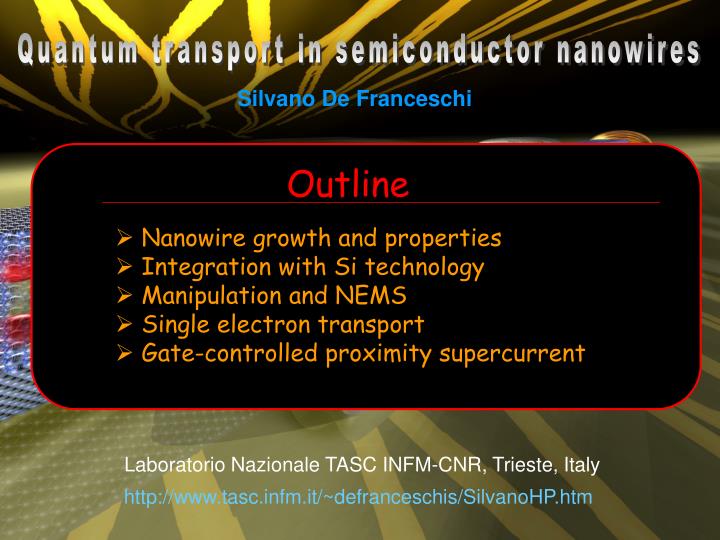
Outline. Nanowire growth and properties Integration with Si technology Manipulation and NEMS Single electron transport Gate-controlled proximity supercurrent. Quantum transport in semiconductor nanowires. Silvano De Franceschi. Laboratorio Nazionale TASC INFM-CNR, Trieste, Italy.

E N D
Outline • Nanowire growth and properties • Integration with Si technology • Manipulation and NEMS • Single electron transport • Gate-controlled proximity supercurrent Quantum transport in semiconductor nanowires Silvano De Franceschi Laboratorio Nazionale TASC INFM-CNR, Trieste, Italy http://www.tasc.infm.it/~defranceschis/SilvanoHP.htm
Semiconductor nanowires • Key features: • nanoscale diameter • (few to 100 nm) • High aspect ratio • (1-100 micron long) • Versatility in composition Catalytic (VLS) crystal growth liquid Au-InP eutect vapor gold particle nanowire time
Possible nanowire structures hollow heterojunctions coaxial p-n junctions
Before growth InP wire on SiO2 • Zinc Blende • [111] direction [111] 10 nm
Hollow core wall wall 200 nm 5 nm Zinc Blende crystal structure InP Tubes Bakkers et al., JACS2003, 125, 3440
InP 50 nm GaP 600 Counts 400 200 0 0 10 20 Position (nm) P Ga In Coaxial wires Group III modulation
GaAs GaAs Au GaAs 100 nm GaP GaP GaP GaP GaAs GaP Heterojunctions GaP: 1.8 nm/sec GaAs: 5.0 nm/sec Group V modulation
Heterostructures nanowires (Chemical beam epitaxy, MOVPE) InAs InP InAs (001) Björk et al., NanoLetters 2, 87 (2002) (Samuelson’s group – Lund) • Almost atomically sharp interfaces • No strain-induced dislocations (stress can relax at the surface)
5 m Vsd (mV) InP More recently: epitaxial InP on Si! [See also Mårtensson et al., Nano Letters 4, 1987 (2004)] • Integration of III-V devices with Si technology Ge Epitaxial InP wires on Ge HR TEM The InP/Ge heterointerface provides a low-resistance Ohmic contact between wire and substrate I (mV) I Conducting AFM
Source Source p Gate n III-V Drain Drain Silicon Silicon III-V devices on silicon Vertical transistor Nano LED NANOWIRE LED: Gudiksen et al., Nature (2002) Enhanced speed Enhanced transconductance Small footprint NANOWIRE LASERS: Johnson et al., Nature Materials (2002) Duan et al., Nature (2003)
Nanowire biosensors More on Nanowire devices… Cui et al., Science 293, 1289 (2001). Nanowire trees Nanowire optical waveguides Dick et al., Nature Materials 3, 380 (2004). Law et al., Science 305, 1269 (2004).
Electrically-driven nanowire cantilever Nanowire “string”
After wet etching… following subsequent AFM manipulation….
Vs-d Vgate Low-temperature transport in semiconductor NWs SiO2 Si p+ InP & InAs n-type nanowires Diameter: 25 – 140 nm Length: 2 – 20 mm • Device fabrication: • wires deposited on p-type Si wafer with a 250-nm-thick surface oxide • Ti/Al contacts defined by e-beam lithography
Single-electron tunneling in InP nanowires +4 VSD [mV] 0 L~600 nm T~350 mK Ec~1 meV -4 Typical island size: ~100 nm 0 -100 -200 -300 -400 Vgate [mV] • Differential conductance (black: low, white: high); • Many diamonds visible. Not so regular, but very stable and reproducible. • Single & Multiple(probably two)-island behavior
InP-nanowire quantum dot: Zeeman spin splitting DE gmBB V (mV) N+1 N B = 0.5 T B = 31 mT Vg (mV) Vg (mV) g = 1.5 ± 0.2
source drain top gates Side gates Tunable Quantum Dots Few-electron quantum dots in InAs/InP nanowires InAs QD Björk et al., Nano Lett. 4, 1621 (2004) InP barriers
Low contact resistance => no Coulomb blockade Superconducting contacts => Proximity effect N (1-D or 0-D) S S For T < 1.2 K Superconductor Nanowire Superconductor Only a few experiments done on similar hybrid systems based on carbon nanotubes: Kasumov et al, Science 284 (’99) Morpurgo et al., Science 286 (’99) Buitelaar et al., PRL 89 (’02); PRL 91 (‘03) Jarillo-Herrero et al. (unpublished)
InAs nanowire devices Ti(10 nm)/Al(120 nm) InAs [100] 4-point contacts: SiO2 Si (p+) Vgate Device resistances: 0.4 – 4 K Lsd W f source Lsd = 60 – 500 nm drain
2D0/e B=0 Enhanced conductance for 2D0<V<2D0 High contact transparency (T~75%) Supercurrent in InAs nanowires IC = 136 nA RN = 417 W ICRN = 60 mV ~ D0/e (90 % device yield!) T = 40 mK Hysteretic behavior due to strong capacitive coupling between source and drain
Multiple Andreev reflection Normal Super T < Tc D m m D S N Peaks at Vn=2D0/ne: V1=2D0/e V2= 2D0/2e V3= 2D0/3e Andreev reflection in a S-N junction From 3 different devices:
Field-effect control of the supercurrent 0 30 kW Supercurrent fluctuations correlate with normal-state universal conductance fluctations Electron transport through the nanowire is diffusive and phase coherent => mesoscopic Josephson junctions First Josephson Field Effect Transistors: Takayanagi et al., PRL (1985). Kleinsasser et al., Appl. Phys. Lett. (1989). Nguyen et al., Appl. Phys. Lett. (1990).
DV=10 mV AC Josephson effect: Rf irradiation => Shapiro steps DV= (/2e)wrf = 2.068 mV for 1 GHz “Quantized voltage steps depending on RF frequency”
Shapiro steps: rf-power dependence (b) (c) (a) wrf = 2 GHz wrf = 4 GHz wrf = 5 GHz IC DIN=1 DIN=2 DIN=3 DIN=4 DIN ~ N-th order Bessel function with IC,fit = 34 nA > IC,exp = 26 nA
References Epitaxial III-V nanowires on Ge [Nature Materials 3, 769 (2004)] Nanowire SET [Appl. Phys. Lett. 83, 344 (2003)] Nanowire JOFET [Science 309, 272 (2005)] Nanowire SQUID [unpublished] Collaborators Philips Eindhoven: Jorden van Dam Floris Zwanenburg L. Gurevich Yong-Joo Doh Leo Kouwenhoven Erik Bakkers Aarnoud Roest Lou-Fe Feiner