Download
1 / 24
260 likes | 496 Views
HfO 2 thin films prepared by sol-gel method A.Barău 1 , M.Gartner 1 , M.Anastasescu 1 , V.S.Teodorescu 2 , M.G.Blanchin 3, J.Tardy 4 and M.Zaharescu 1 1 Institute of Physical Chemistry "Ilie Murgulescu" - Roumanian Academy 202 Splaiul Independentei, 060021 Bucharest, ROUMANIA

E N D
HfO2 thin films prepared by sol-gel method A.Barău1, M.Gartner1, M.Anastasescu1, V.S.Teodorescu2, M.G.Blanchin3, J.Tardy4 and M.Zaharescu1 1Institute of Physical Chemistry "Ilie Murgulescu" - Roumanian Academy 202 Splaiul Independentei, 060021 Bucharest, ROUMANIA 2National Institute of Material Physics, 105 bis Atomistilor Street, 077125 Bucharest-Măgurele, ROUMANIA 3Universite Claude Bernard Lyon 1, 43 Boulevard du 11 Novembre 1918, 69622 Villeurbane CEDEX-FRANCE 4Ecole Centrale de Lyon , LEOM , 36 avenue Guy de Collongue, 69134 Ecully, FRANCE _____________________________________________________________________________________________
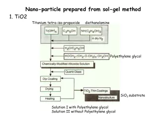
Objectives • The preparation of HfO2 thin films by sol-gel method • The establishing the correlation between the way of preparation and optical and structural properties of these materials.
Why the HfO2 ? • HfO2 properties: • High thermal and chemical stability • High thermodinamic stability in contact with silicon • High refractive index (~ 2.00) • Large band gap (5.86 eV) • High dielectric constant (K ≈ 15-50) • High density (9.86 g/cm2) • Stable structure – SGP- (14) monoclinic : symmetry P121/c1 • (a = 0.51156nm, b= 0.51722 nm, c= 0.52948 nm , b = 99,2)
Why the HfO2 ? • Possible applications: • in micro and optoelectronics: • - material for replacing SiO2 in metal/oxide/semiconductor (MOS) devices • - optical coatings when high optical damage thresholds are needed • - waveguide fabrication • as material for nanofiltration membranes and • films with high pencil hardness (over 9H) and hydophobicity
Why the HfO2 ? Methods of film preparation (literature): • Sputtering (Kang et al – 2000, Lee et al – 2000) • Chemical vapor deposition - thermal (Balog et al – 1979 Lee et al – 2000) - plasma enhenced (Choi et al – 2002) - UV photo induced (Fang et al – 2004) • Pulsed layer deposition (Esang et al – 2004) • Atomic layer deposition (Zhang and Solanski – 2001, Ferari et al - 2004, Boher et al – 2004, Aarik et al – 2004)
Why the HfO2 ? Methods of film preparation (literature): • Sol-gel methods: • - starting with HfCl4 in ethanol (Nishide et al – 2000, • Shimada et al – 2002, Yu et al – 2003) • - starting with HfCl4 in 1-methoxy-2 propanol (Blanc et al – 2000) • - starting with HfCl4 in water, via hafnia hydroxide formation and peptization with formic/oxalic acid (Takahashi and Nishide – 2004, Nishide et al – 2005) • - starting with HfOCl2 in ethanol (Gonçalves et al – 2004) • - starting with Hf(OC2H5)4 and Acac (Villanueva-Ibanez et al – 2003)
Experimental: Film preparation • •The reagents: • - hafnium ethoxide Hf(OC2H5)4 (Alfa Aesar) as HfO2 source, • - acetyl acetone AcAc (Fluka) as stabilisator and • - absolute alcohol p.a. (Merck) as solvent. • Molar ratio: Hf(OC2H5)4/Acac = 1. • •Solution preparation: mixing of the reagents in N2 atmosphere at 1000C for two hours. • Synthesis were also performed starting with Hf-acetyl-acetonate or Hf-chloride, that allows working in ambinet atmosphere.
Experimental: Film preparation • Film deposition: - substrates: silicon wafer; - deposition method: - dip-coating (5-8 cm/min withdraw speed), - spinning (5000 rpm) Before deposition the native SiO2 was removed in HF •Film densification: - 10 min at 100C and 30 min at 450o or 600oC with a heating rate of 1C/min. - For the multi-layered films, the same thermal treatment was applied, after each deposition
Experimental: Films characterization • Spectroellipsometric (SE) measurements in the 300-700 nm spectral range • TEM (Topcon 00B and a Jeol 200 CX electron microscopes working at 200kV) • AFM (MultiMode SPM equipment - Instrument Veeco Metrology Group) • RBS (4+He:E = 1.5 MeV) Preliminary electrical measurements were performed.
Results obtained Spectroellipsometry Spectroellipsometric results on samples obtained by dip-coating, thermally treated at 450oC • the refractive indexes (n),the thickness of the samples (d) and the volume fractions of film components were obtained from the best fit of the SE experimental data with a multilayer and multicomponent Bruggemann-EMA model • ►The thickness of one layer deposition by spinning was 200 Å
Results obtained Spectroellipsometry (a) (b) The thickness (a) and refractive indexes (n) of the samples with 1-3 layers (b) from spectroellipsometric results ►by multilayer deposition the thickness of the films increases linearly ►due to the densification by the repetitive thermal treatments the refractive index of the film increases
Results obtained Atomic Force Microscopy • Very low RMS roughness between 0.7 and 1.5 nm • Very small surface roughness • (~1 and ~1.5 nm) Dip coated film – one layer dried
Results obtained Atomic Force Microscopy dried dried annealed 450oC Annealed 450oC • Maximum profile roughness • up to 10 nm • Large surface roughness Spin coated films – one layer
Results obtained Rutherford Backscattering spectrometry Dip coated films Spin coated films ►No deformation of the Hf and Si peaks ►Dissymmetry and Deformation of Hf and Si peaks:
Results obtained Transmission Electron Microscopy Plan view TEM image and SAED pattern of the HfO2 film dried at 100oC and then annealed at 150oC (to be stable in the microscope) • Amorphous structure with an non-uniform density in the nanometric scale
Results obtained Transmission Electron Microscopy Plan view TEM image and SAED pattern of the HfO2 film annealed at 450oC • The structure is still amorphous with a beginning of crystallization
Results obtained Transmission Electron Microscopy Plan view HRTEM image of the HfO2 film annealed at 600oC • The crystallization of the monoclinic HfO2 is observed. • The crystallites are like a sponge. • Pores with an average dimension of about 4.6 nm are observed.
Results obtained Transmission Electron Microscopy Thermally treated at 450oC film Thermally treated at 6000C High resolution XTEM image of the cross section of the HfO2 filmsdeposited by dip-coating
Results obtained Electrical Properties I-V curves variation and mobility for the HfO2 sol-gel films thermally treated at 450oC • Low operation voltage • Almost no hysteresis • Low threshold voltage • Good mobility
Results obtained Electrical Properties • The low operation voltage was assigned to the very thin dielectric film • Improved stability was correlated to the porous nature of HfO2 with air inclusion • The extremely low threshold voltage (VT ~ -0.4V) and high mobility are related to the very smooth surface of the film
Conclusions • The possibility to obtain HfO2 thin films by the sol-gel method was confirmed • The films have shown a dependence of the refractive indices and of the thickness on the number of depositions and the thermal treatments applied • The structural evolution with the thermal treatment was established • Preliminary electrical measurements were performed
Acknowledgments The work was realized as a collaboration (UMR No. 5586) of the Institute of Physical Chemistry of the Romanian Academy, Bucharest, Romania with the Laboratoire de Physique de la Matière Condensée et Nanostructures, Lyon, France, as a part of the existing cooperation agreement between the Romanian Academy and CNRS-France. The work was also supported by the Romanian Academy with Grant No. 41/2005.