Download
1 / 2
20 likes | 122 Views
Seeing Crystal Nuclei with Nanodiffraction Paul M. Voyles , University of Wisconsin-Madison, DMR 0905793.

E N D
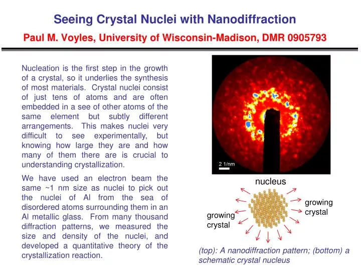
Seeing Crystal Nuclei with NanodiffractionPaul M. Voyles, University of Wisconsin-Madison, DMR 0905793 Nucleation is the first step in the growth of a crystal, so it underlies the synthesis of most materials. Crystal nuclei consist of just tens of atoms and are often embedded in a see of other atoms of the same element but subtly different arrangements. This makes nuclei very difficult to see experimentally, but knowing how large they are and how many of them there are is crucial to understanding crystallization. We have used an electron beam the same ~1 nm size as nuclei to pick out the nuclei of Al from the sea of disordered atoms surrounding them in an Al metallic glass. From many thousand diffraction patterns, we measured the size and density of the nuclei, and developed a quantitative theory of the crystallization reaction. nucleus growing crystal growing crystal (top): A nanodiffraction pattern; (bottom) a schematic crystal nucleus
Seeing Crystal Nuclei with NanodiffractionPaul M. Voyles, University of Wisconsin-Madison, DMR 0905793 Electron microscopes like the one used for this research project are used to measure the structure and composition of a wide variety of nanomaterials and nano-devices. This creates a need for education of students and researchers in these cutting edge characterization techniques. We have contributed to meeting this need by developing the Electron Microscopy Database (tem.msae.wisc.edu/emdb/), a web database of example data sets from electron microscopy for teaching and learning. In the past year, data sets covering sub-Ångstrom resolution imaging and composition mapping by electron and x-ray spectroscopy have been added to the database. 2 nm EMdb records: (top) a dislocation in ZnO; (bottom) EDS composition maps of a magnetic tunnel junction