Download
1 / 17
170 likes | 345 Views
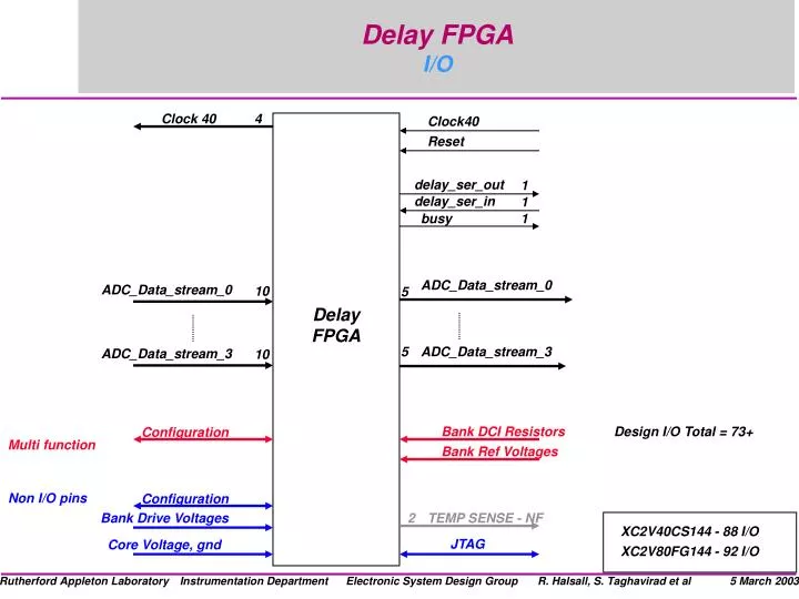
Delay FPGA I/O. Clock 40. 4. Clock40. Reset. delay_ser_out. 1. delay_ser_in. 1. busy. 1. ADC_Data_stream_0. ADC_Data_stream_0. 10. 5. Delay FPGA. 5. ADC_Data_stream_3. ADC_Data_stream_3. 10. Bank DCI Resistors. Design I/O Total = 73+. Configuration. Multi function.

E N D
Delay FPGAI/O Clock 40 4 Clock40 Reset delay_ser_out 1 delay_ser_in 1 busy 1 ADC_Data_stream_0 ADC_Data_stream_0 10 5 Delay FPGA 5 ADC_Data_stream_3 ADC_Data_stream_3 10 Bank DCI Resistors Design I/O Total = 73+ Configuration Multi function Bank Ref Voltages Non I/O pins Configuration Bank Drive Voltages 2 TEMP SENSE - NF XC2V40CS144 - 88 I/O JTAG Core Voltage, gnd XC2V80FG144 - 92 I/O
Delay FPGAFunction 4 phases XC2V40-CS144 CLOCK OUT 0 CLOCK - 40 MHz DCM 0 IOB IOB 5 Slices 5 Slices REG DCI 1 10 SHIFT REG REG DATA OUT 0 REG REG BLOCK RAM 0 10 Slices DPM Counter 2.5/3.3V I/O? 4 phases 1.5/1.8/2.5/3.3V I/O? CLOCK OUT 3 DCM 3 IOB IOB 5 Slices 5 Slices REG DCI 4 10 10 SHIFT REG DATA OUT 3 REG REG REG BLOCK RAM 3 10 Slices DPM Control Counter Clock RESET Serial In CONTROL Serial Out busy
CMS Tracker FED FirmwareFront End FPGA I/O Clock40 3 Clock40 LVDS adc enables 18 Opto Rx 6 Frame_Sync_out Frame_Sync_In 8 2 x Temp Sense Readout_Sync_out 4 DAC Serial Readout_Sync_In Config_out (Config_Monitor_Out) delay_ser_out Config_In (Config_Monitor_In) 3 FE - BE I/O 12 signals Front End FPGA delay_ser_in 3 Monitor_in (DCM Reset) busy 3 Monitor_out (Synch Reset) ADC_Data_stream_0 5 4 Data_stream ADC_Data_stream_11 5 Full Flags 3 Configuration Bank DCI Resistors VBatt Power down JTAG Bank Voltages Temp Sense Core Voltage
CALICE FirmwareFront End FPGA I/O Clock 40 3 Clock40 adc control x dac control x Frame_Sync_out Temp monitor Frame_Sync_In (Trigger) Readout_Sync_out Readout_Sync_In Config_out (Config_Monitor_Out) Config_In (Config_Monitor_In) FE - BE I/O 12 signals LVDS I/O Front End FPGA Monitor_in (DCM Reset) Monitor_out (Synch Reset) ADC_Data_stream_0 1 4 Data_stream ADC_Data_stream_11 1 Full Flags 3 Configuration Bank DCI Resistors VBatt Power down JTAG Bank Voltages Temp Sense Core Voltage
CMS Tracker FED FPGA Firmware Back End FPGA I/O Frame_Sync_out0 Clock40 Frame_Sync_in 0 DCM Reset Readout_Sync_out0 Serial 3 Readout_Sync_In0 6 spare VME Sync Reset VME SLINK 32 12 FE0 DCM Reset out 0 2 control Load_Monitor_In 0 1 interrupt Load_monitor_out 0 TTCrx TTS 4 Data_stream0 J0 4 pairs TTC/S Spare & Test Trig Single ended DCI J0 3 pairs Frame_Sync_out 7 Frame_Sync_in 7 SLINK64 64 SLINK Readout_Sync_out 7 J2 32 + 13 pairs Control Readout_Sync_In 7 12 Sync Reset FE7 ADDR/CNTRL DCM Reset out 7 18 Load_monitor_In 7 DATA IN QDR SSRAM 18 x2 QDR Common Address Load_monitor_out 7 18 DATA OUT 4 Data_stream 7 8 x 2 Clock40 Bank DCI Resistors LVDS Full flags 3 Temp Flag ef, pf & ff ‘I2C’ LM82 Temp Sense diode Bank Voltages BSCAN Core Voltage
CMS Tracker FED FPGA Firmware Back End FPGA Overview Clock40 VME Channel Link x1 640 MHz Clock Management x2 Clock40 TTC x8 Clock40 J0 8 Clock40 FE 3 SLINK LVDS 32 Control 3 VME SLINK Serial I/O VME SLINK Data 64 8 interrupt 6 spare 8x 8 Frame_Syncs 8 Readout_Syncs 8 CONTROL Load_monitor 64 2 x 18 Front End 8 Data Out Synch/DCM Reset 160 MHz 2 FF/PF Flags QDR QDR SSRAM x2/x4 burst 8x Lengths, Pointers 9 Pipelined Address Generator TTC Rx 18+4 Fill/run/freeze Address TTX TTS 160MHz FF, PF, busy Control Data 4 Pipelined Data Mux Data_stream 0 64 2 x 18 Data In 160 MHz 4 160 MHz 80 MHz Data_stream 7
CMS Tracker FED FPGA Firmware Back End FPGA Control Block VME Serial I/O Serial Interface Header Control SLINK P2p Serial Load_Monitor 0..7 Load_Monitor 0..7 FS in 0..7 Frame Sync Interface FS out 0..7 RS in 0..7 QDR ADDR/CTRL Readout Sync Interface QDR Addr RS out 0..7 Header Generation Data tap 0..X SLINK SLINK SLINK-VME SLINK Data 0..63 QDR Data TTC Interface TTC 0..9 DIagnostics FE FPGA FF/PF 0..1 Flow Control Interface TTS 0..X Resets
CMS Tracker FED FPGA Firmware Back End FPGA Control Block Serial Detect Compare CTRL fs_strobe, status= good, some header errors, arrival time error, fatal error FS in 0..7 reset, freeze FIFO 512x80 HEADER fs_fifo_empty, fs_fifo_full, fifo_data=median header+status 8x Serial Data, markers & control data DPM 1K circular buffer VME SERIAL CSR
Readout Sync Serial Detect CTRL BUS rs_strobe, status= good, arrival time error, fatal error RS in 0..7 reset, freeze,readout_next RS out 0..7 FIFO 1K Address Gen Total_length_fifo_empty, total_length_fifo_full, fifo_data= total length FIFO 8K fifo_data= 8x sub_lengths FIFO 8K fifo_data= 8x pointer_offsets FIFO 8K HEADER copy_fifo_empty, copy_fifo_full, fifo_data= sub_lengths 8x Serial Data, markers & control data DPM 1K circular buffer VME Serial
Flow Control core VME soft reset Addr Gen FIFO FF Internal FIFO FF Internal Freeze TTS ERROR Latch FE FPGA FF Addr Gen FIFO PF Internal FIFO PF TTS BUSY FE FPGA PF Addr GEN FF Addr GEN Controls Fill Flow Control Internal FIFO EF RS Controls Internal Freeze Fill event SLINK CTRL Busy Simplest flow control; Halt on any buffer full Busy on any buffer partially full Empty Flow Control Addr GEN EF Addr GEN Busy Readout event Internal Freeze Diagnostic Event Logger Circular Buffers Serial Time stamped Control Registers
TTC Interface TTC Interface CTRL BUS ttc_strobe TTC 0..9 reset, freeze Bx,Ex FIFO 1K Header Em Hdr FIFO 1K DPM 1K VME Serial
VME FPGA Temp Sensor EEPROM I2C Temp Sense CSR VME INT System ACE Address/control data SYS ACE Clock Management BE FPGA Serial BE FPGA Parallel Int XTAL J0 32 wait Clock 40 Serial I/O control data burst 6 spare BE FPGA
VME-BE-Parallel VME-SLINK Interface data DPM 1K wait burst 32 SLINK Data from BE FPGA ‘VME’ BUS lengths FIFO 1K QDR Event Data moved in blocks into DPM Burst transfer over VME Wait on software handshake before continuing Double buffered
VME-BE-Serial Serial I/O Engine DPM 1K Serial in 0..7 Serial out 0..7 Output ‘VME’ BUS DPM 1K Input
CMS Tracker FEDSystem Timing Frame Sync In 256+12 #2234 Header Data ADC Output Frame Sync Median header+ Status Message Frame Sync Out Accept/abort Handshake Message Frame Sync In #2233 Length Readout Sync Out Processed Message #2220 Next/delete #2221 Readout Message Readout Message Readout Sync In #2219 #2220 #2221 Data Burst Data Burst Data Burst Data NB Frame Sync In - Abort/Accept not used, auto accepts. Readout Sync In - delete not used.
CMS Tracker FED Back End FPGA #FFFFF Event N+1 Event N+1 Event N+1 Write Ptr 7 FE 7 Write Ptr 7 Write Ptr 7 Write Ptr 2 Event N Write Ptr 2 Write Ptr 2 Write Ptr 1 FE 1 Write Ptr 1 Write Ptr 0 Write Ptr 1 FE 0 Write Ptr 0 Write Ptr 0 Read Ptr Event N-1 Event N-1 Event N-1 Read Ptr Read Ptr #00000 T0 T1 T2
CMS Tracker FED - Back End FPGA Floorplan Die Package VME FE_FPGA_Inputs SLINK QDR Same frame 456 & 676 ? XC2V1000FG456 - 324 I/O Clocks XC2V1500FG676 - 396 I/O XC2V2000FG676 - 456 I/O XC2V3000FG676 - 484 I/O