Download
1 / 43
430 likes | 491 Views
IKI10201 07-Storage Components. Bobby Nazief Semester-I 2005 - 2006. The materials on these slides are adopted from: CS231’s Lecture Notes at UIUC, which is derived from Howard Huang’s work and developed by Jeff Carlyle; Prof. Daniel Gajski’s transparency for Principles of Digital Design.

E N D
IKI10201 07-Storage Components Bobby Nazief Semester-I 2005 - 2006 • The materials on these slides are adopted from: • CS231’s Lecture Notes at UIUC, which is derived from Howard Huang’s work and developed by Jeff Carlyle; • Prof. Daniel Gajski’s transparency for Principles of Digital Design.
Road Map Logic Gates &Flip-flops 3 Boolean Algebra 3 6 Finite-StateMachines 6 4 Logic DesignTechniques Sequential DesignTechniques CombinatorialComponents StorageComponents 2 Binary Systems& Data Represent. 7 5 8 Register-TransferDesign 8 Generalized FSM ProcessorComponents 9
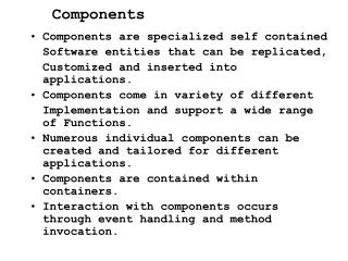
Storage components • Storage components store data & perform some simple operations. • Storage components include: • registers • counters • register files • memories • queues • stacks • Together with combinatorial components, storage components are used for construction of datapaths & controllers, which are main subsystems of modern processors.
Registers • Flip-flops are limited because they can store only one bit. • We had to use two flip-flops for our module-3 up/down counter example. • Most computers work with integers and single-precision floating-point numbers that are 32-bits or 64-bits long. • A register is an extension of a flip-flop that can store multiple bits. • Registers are commonly used as temporary storage in a processor. • They are faster and more convenient than main memory. • More registers can help speed up complex calculations.
A basic register • Basic registers are easy to build. We can store multiple bits just by putting a bunch of flip-flops together! • A 4-bit register is on the right, and its internal implementation is below. • This register uses D flip-flops, so it’s easy to store data without worrying about flip-flop input equations. • All the flip-flops share a common CLK signal. • Qi = Ii during the positive transition of CLK
Register w/ asynchronous set (preset) & reset (clear) • Basic registers can be enhanced by adding different control signals. • E.g., we can add Set & Reset signals to set or reset independent of the clock signal: • the register could be reset (Qi = 0) by pulling the Reset input to 0 for a short period of time • the register could be set (Qi = 1) by pulling the Set input to 0 for a short period of time
Register w/ parallel load • Control the data-loading by adding a Load (LD) or Enable signal. • When LD = 0, the flip-flop inputs are Q3-Q0, so each flip-flop just keeps its current value. • When LD = 1, the flip-flop inputs are D3-D0, and this new value is “loaded” into the register.
4-bit serial-in/parallel-out shift-right registers • The data stored in the register could be shifted one bit in the right direction when the control signal Shift is equal to 1.
Serial data transfer • One application of shift registers is converting between “serial data” and “parallel data.” • Computers typically work with multiple-bit quantities. • ASCII text characters are 8 bits long. • Integers, single-precision floating-point numbers, and screen pixels are up to 32 bits long. • But sometimes it’s necessary to send or receive data serially, or one bit at a time. Some examples include: • Input devices such as keyboards and mice. • Output devices like printers. • Any serial port, USB or Firewire device transfers data serially. • Recent switch from Parallel ATA to Serial ATA in hard drives.
Receiving serial data • To receive serial data using a shift register: • The serial device is connected to the register’s SI input. • The shift register outputs Q3-Q0 are connected to the computer. • The serial device transmits one bit of data per clock cycle. • These bits go into the SI input of the shift register. • After four clock cycles, the shift register will hold a four-bit word. • The computer then reads all four bits at once from the Q3-Q0 outputs. serial device computer
Sending data serially • To send data serially with a shift register, you do the opposite: • The CPU is connected to the register’s D inputs. • The shift output (Q3 in this case) is connected to the serial device. • The computer first stores a four-bit word in the register, in one cycle. • The serial device can then read the shift output. • One bit appears on Q3 on each clock cycle. • After four cycles, the entire four-bit word will have been sent. computer serial device
1 10 00 1 1 01 11 1 Introducing counters • Counters are a specific type of registers that incorporate an incrementer. • The state, or the flip-flop values themselves, serves as the “output.” • The output value increases by one on each clock cycle. • After the largest value, the output “wraps around” back to 0. • Using two bits, we’d get something like this:
10 00 01 11 0 0 1 0 1 1 1 0 Up/down counters • Here’s the complete state diagram and state table for this circuit. • Make sure you know how to come up with these – this is a typical sequential design problem!
Asynchronous Counters • Each FF in synchronous counters changes its output at the same time • Each FF in asynchronous counters changes its output at different times • Advantage of asynchronous counters is low cost (less gates) • Weakness of asynchronous counters is longer delays
Register Files • Register-file is a set of registers combined into 2-dimensional array • used as fast temporary storage
Random access memory (RAM) • Sequential circuits all depend upon the presence of memory. • A flip-flop can store one bit of information. • A register can store a single “word,” typically 32-64 bits. • Random access memory, or RAM, allows us to store even larger amounts of data. Today we’ll see: • The basic interface to memory. • How you can implement static RAM chips hierarchically.
A RAM should be able to: • - Store many words, one per address • - Read the word that was saved at a particular address • - Change the word that’s saved at a particular address Introduction to RAM • Random-access memory, or RAM, provides large quantities of temporary storage in a computer system. • Remember the basic capabilities of a memory: • It should be able to store a value. • You should be able to read the value that was saved. • You should be able to change the stored value. • A RAM is similar, except that it can store many values. • An address will specify which memory value we’re interested in. • Each value can be a multiple-bit word (e.g., 32 bits). • We’ll refine the memory properties as follows:
Picture of memory • You can think of computer memory as being one big array of data. • The address serves as an array index. • Each address refers to one word of data. • You can read or modify the data at any given memory address, just like you can read or modify the contents of an array at any given index. • If you’ve worked with pointers in C or C++, then you’ve already worked with memory addresses.
2k x n memory ADRS OUT DATACS WR k n n Block diagram of RAM • This block diagram introduces the main interface to RAM. • A Chip Select, CS, enables or disables the RAM. • ADRS specifies the address or location to read from or write to. • WR selects between reading from or writing to the memory. • To readfrom memory, WR should be set to 0. OUT will be the n-bit value stored at ADRS. • To write to memory, we set WR = 1. DATA is the n-bit value to save in memory. • We refer to this as a 2k x n memory. • There are k address lines, which can specify one of 2k addresses. • Each address contains an n-bit word.
2k x n memory ADRS OUT DATACS WR k n n Reading RAM • To read from this RAM, the controlling circuit must: • Enable the chip by ensuring CS = 1. • Select the read operation, by setting WR = 0. • Send the desired address to the ADRS input. • The contents of that address appear on OUT after a little while. • Notice that the DATA input is unused for read operations.
2k x n memory ADRS OUT DATACS WR k n n Writing RAM • To write to this RAM, you need to: • Enable the chip by setting CS = 1. • Select the write operation, by setting WR = 1. • Send the desired address to the ADRS input. • Send the word to store to the DATA input. • The output OUT is not needed for memory write operations.
Static memory • How can you implement the memory chip? • There are many different kinds of RAM. • We’ll start off discussing static memory, which is most commonly used in caches and video cards. • Later wemention a little about dynamic memory, which forms the bulk of a computer’s main memory. • Static memory is modeled using one latch for each bit of storage. • Why use latches instead of flip flops? • A latch can be made with only two NAND or two NOR gates, but a flip-flop requires at least twice that much hardware. • In general, smaller is faster, cheaper and requires less power. • The tradeoff is that getting the timing exactly right is a pain.
Dynamic memory • Dynamic memory is built with capacitors. • A stored charge on the capacitor represents a logical 1. • No charge represents a logic 0. • However, capacitors lose their charge after a few milliseconds. The memory requires constant refreshing to recharge the capacitors. (That’s what’s “dynamic” about it.) • Dynamic RAMs tend to be physically smaller than static RAMs. • A single bit of data can be stored with just one capacitor and one transistor, while static RAM cells typically require 4-6 transistors. • This means dynamic RAM is cheaper and denser—more bits can be stored in the same physical area.
Memory cell • To start, we can use one latch to store each bit. A one-bit RAM cell is shown here. • Since this is just a one-bit memory, an ADRS input is not needed. • Writing to the RAM cell: • When CS = 1 and WR = 1, the latch control input will be 1. • The DATA input is thus saved in the D latch. • Reading from the RAM cell and maintaining the current contents: • When CS = 0 or when WR = 0, the latch control input is also 0, so the latch just maintains its present state. • The current latch contents will appear on OUT.
My first RAM • We can use these cells to make a 4 x 1 RAM. • Since there are four words, ADRS is two bits. • Each word is only one bit, so DATA and OUT are one bit each. • Word selection is done with a decoder attached to the CS inputs of the RAM cells. Only one cell can be read or written at a time. • Notice that the outputs are connected together with a single line!
The “C” means “conflict.” Connecting outputs together • In normal practice, it’s bad to connect outputs together. If the outputs have different values, then a conflict arises. • The standard way to “combine” outputs is to use OR gates or muxes. • This can get expensive, with many wires and gates with large fan-ins.
Those funny triangles • The triangle represents a three-state buffer. • Unlike regular logic gates, the output can be one of three different possibilities, as shown in the table. • “Disconnected” means no output appears at all, in which case it’s safe to connect OUT to another output signal. • The disconnected value is also sometimes called high impedance or Hi-Z.
Connecting three-state buffers together • You can connect several three-state buffer outputs together if you can guarantee that only one of them is enabled at any time. • The easiest way to do this is to use a decoder! • If the decoder is disabled, then all the three-state buffers will appear to be disconnected, and OUT will also appear disconnected. • If the decoder is enabled, then exactly one of its outputs will be true, so only one of the tri-state buffers will be connected and produce an output. • The net result is we can save some wire and gate costs. We also get a little more flexibility in putting circuits together.
A 4 x 4 RAM • DATA and OUT are now each four bits long, so you can read and write four-bit words.
16 8 8 Bigger RAMs from smaller RAMs • We can use small RAMs as building blocks for making larger memories, by following the same principles as in the previous examples. • As an example, suppose we have some 64K x 8 RAMs to start with: • 64K = 26 x 210 = 216, so there are 16 address lines. • There are 8 data lines.
8 16 8 Making a larger memory • We can put four 64K x 8 chips together to make a 256K x 8 memory. • For 256K words, we need 18 address lines. • The two most significant address lines go to the decoder, which selects one of the four 64K x 8 RAM chips. • The other 16 address lines are shared by the 64K x 8 chips. • The 64K x 8 chips also share WR and DATA inputs. • This assumes the 64K x 8 chips have three-state outputs.
8 16 8 Analyzing the 256K x 8 RAM • There are 256K words of memory, spread out among the four smaller 64K x 8 RAM chips. • When the two most significant bits of the address are 00, the bottom RAM chip is selected. It holds data for the first 64K addresses. • The next chip up is enabled when the address starts with 01. It holds data for the second 64K addresses. • The third chip up holds data for the next 64K addresses. • The final chip contains the data of the final 64K addresses.
8 16 11 1111 1111 1111 1111 (0x3ffff) to 11 0000 0000 0000 0000 (0x30000) 10 1111 1111 1111 1111 (0x2ffff) to 10 0000 0000 0000 0000 (0x20000) 01 1111 1111 1111 1111 (0x1ffff) to 01 0000 0000 0000 0000 (0x10000) 00 1111 1111 1111 1111 (0x0ffff) to 00 0000 0000 0000 0000 (0x00000) 8 Address ranges
8 8 16 8 8 Making a wider memory • You can also combine smaller chips to make wider memories, with the same number of addresses but more bits per word. • Here is a 64K x 16 RAM, created from two 64K x 8 chips. • The left chip contains the most significant 8 bits of the data. • The right chip contains the lower 8 bits of the data.
Simple datapath • Datapath are used for temporary variable storage & operation execution • To control the operation, control word is used: • Input select: select ALU’s A-input • ALU controls: define the type of operations (Add, Subtract, ...) • Accumulator controls: define the type of data operations within accumulator (Shift, Rotate, ...)
Control unit • Control unit is a sequential circuit that controls datapath’s operations • it receives computer’s instructions (our programs) and status signals as input • it generates the control words and other control outputs