Download

1 / 39
400 likes | 565 Views
The Digital Logic Level. Chapter 3. Memory. Latches To create a 1-bit memory, we need a circuit that somehow remembers previous input values. SR Latch Inputs: S (set), R(Reset) Outputs: Q and Q

E N D
The Digital Logic Level Chapter 3
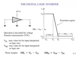
Memory • Latches • To create a 1-bit memory, we need a circuit that somehow remembers previous input values. • SR Latch • Inputs: S (set), R(Reset) Outputs: Q and Q • Unlike a combinational circuit, the outputs of the latch are not uniquely determined by the current inputs.
Latches (1) • No Change • Set to 1 • Clear to 0 • Indeterminate S R Q(Current) Q(New) 0 0 0 0 0 0 1 1 1 0 0 1 1 0 1 1 0 1 0 0 0 1 1 0 1 1 x ?
Clocked SR Latches (1) • To prevent the latch from changing state except at certain specified times, we modify the circuit below. • This circuit has an additional input, the clock, which is normally 0. • The terms enable and strobe are also used to mean the clock input is 1. • Figure 3-22. A clocked SR latch.
Clocked SR Latches (2) • When R = S = 1, the circuit becomes non-deterministic when both S and R finally return to 0. • The only consistent state for R = S = 1 is Q = Q = 0, but as soon as both inputs return to 0, the latch must jump to one of its two stable states. • If either input drops back to 0 before the other, the one remaining 1 longest wins, because when just one input is 1, it forces the state. • If both inputs return to 0 simultaneously (very unlikely), the latch jumps to one of its stable states at random.
Clocked D Latches D Q 0 0 clear to 0 1 1 set to 1 • The D (Data) latch is a modification of the SR latch. • An SR latch is converted to a D latch by inserting an inverter between S and R and assigning the symbol D to the single input. • To load the current value of D into the memory, a positive pulse is put on the clock line. • This circuit, called a clocked D latch, is a true 1-bit memory. • This circuit requires 11 transistors. • More sophisticated circuits can store 1 bit with only 6 transistors.
Flip-Flops • In many circuits it is necessary to sample the value on a certain line at a particular instant in time and store it. • In a flip-flop, the state transition occurs during the clock transition from 0 to 1 (rising edge) or from 1 to 0 (falling edge) instead when clock is 1 as in a latch. • A flip-flop is edge triggered, whereas a latch is level triggered. • A short pulse can be generated on the rising edge of the clock signal and that pulse can be fed into a D latch, as shown below: • Figure 3-24. (a) A pulse generator.
Flip-Flops • The inverter in the circuit has a small, but non-zero propagation delay through it, that makes the circuit work. • The measurements of voltage at the four points a, b, c and d is as shown: • The signal at b is inverted and delayed slightly. • The signal at c is delayed, but only by the signal propagation time (speed of light) which is negligible. • Figure 3-24. (b) Timing at four points in the circuit.
Flip-Flops • The result of b AND c, is a short pulse, where the width of the pulse, , is equal to the gate delay of the inverter (5 nsec or less). • The output of the AND gate is just this pulse shifted by the delay after the rising edge of the clock, but there is no effect on the pulse width. • In a memory with a 10-nsec cycle time, a 1-nsec pulse telling it when to sample the D line may be short enough. • Figure 3-25. A D flip-flop.
Flip-Flops • Figure 3-26. D latches and flip-flops. • Fig. (a) is a latch whose state is loaded when the clock, CK, is 1. • Fig. (b) is a latch whose clock is normally 1 but which drops to 0 momentarily to load the state from D. • Fig. (c) is a flip-flop that changes state on the rising edge of the clock pulse whereas, in fig. (d), the change of state is on the falling edge. • Many latches and flip-flops have Q as an output, and some have two additional inputs, Set or Preset (force state to Q =1) and Reset or Clear (force state to Q =0).
Memory Organization (1) • A 8-bit memory arrangement is given below • Figure 3-27. An 8-bit register constructed from single-bit flip-flops.
Memory Organization (2) • A memory organization in which individual words can be addressed is as follows. • The example illustrates a memory with four 3-bit words. • Each operation reads or writes a full 3-bit word. • The memory has 8 input lines and 3 output lines. • Three inputs are data: I0, I1, and I2; two are for the address: A0 and A1; and three are for control: CS for Chip Select, RD for distinguishing between read and write, and OE for Output Enable. • The three outputs are for data: O0, O1, and O2. • The 8-bit register requires 20 signals, including power and ground, while the 12-bit memory requires only 13 signals.
Memory Organization (2) • To select this memory chip, external logic must set CS high and also set RD high for read and low for write. • For a read operation, the data input lines are not used, but the word selected is placed on the data output lines. • For a write operation, the bits present on the data input lines are loaded into the selected memory word; the data output lines are not used. • If the OR gates were tied to the data output lines, the chip would try to output data, even on writes, thus interfering with input data. • Thus, OR gates should be connected to the data output lines on reads but disconnected on writes.
Memory Organization (2) • Tri-state devices • In a noninverting buffer, when the control input is high, the buffer acts like a wire, and when it is low, the buffer acts like an open circuit. • Fig. (d) is an inverting buffer, which acts like a normal inverter when control is high and disconnects the output from the circuit when control is low. • Buffers also amplify signals, so they can drive many inputs simultaneously. • Figure 3-29. (a) A noninverting buffer. (b) Effect of (a) when control is high. (c) Effect of (a) when control is low. (d) An inverting buffer.
Memory Chips (1) • The 4x3 memory can be easily extended to 4x8 or to 8x3. • Memory chips are an ideal application for the IC technology as it is suited to making chips whose internal structure is a repetitive two-dimensional pattern. • Two possible organizations for a 4-Mbit memory chip are: 512K x 8 and 4096K x 1. • On some pins, the high voltage causes an action to happen and on others, the low voltage causes the action. • The word asserted means that it is set to cause some action. • A signal named CS is asserted low. • Pins are negated when no action is taken.
Memory Chips (2) • In fig. (a), 19 address lines are needed to address one of the 219 bytes, and eight data lines are needed for loading or storing the byte selected. • The CS (Chip Select) signal is asserted to enable the chip. • The WE (Write Enable) indicates that data is being written rather than being read. • The OE (Output Enable) signal is asserted to drive the output signals. • Figure 3-30. Two ways of organizing a 4-Mbit memory chip
Memory Chips (3) • Internally this chip is organized as a 2048 x 2048 matrix of 1-bit cells. • To address the chip, first a row is selected by putting its 11-bit number on the address pins. • Then the RAS (Row Address Strobe) is asserted. • After that, a column number is put on the address pins and CAS (Column Address Strobe) is asserted. • The chip responds by accepting or outputting one data bit. • Figure 3-30. Two ways of organizing a 4-Mbit memory chip
Memory Chips (4) • Large memories chips are often constructed as n x n matrices that are addressed by row and column. • This organization reduces the number of pins required but makes addressing the chip slower, since two addressing cycles are needed. • To build a memory with 32-bit word from 4096K x 1 chips requires 32 chips in parallel. • These 32 chips have a total capacity of at least 16 MB. • Using 512K x 8 chips requires only four chips in parallel and allows memories as small as 2 MB. • To avoid having 32 chips for memory, most chip manufacturers now have chip families with 4-, 8-, and 16-bit widths.
Memory Chips (5) • Two examples of 512-Mbit chips are given in Fig. 3-31. • These chips have four internal memory banks of 128 Mbit each, requiring two bank select lines to choose a bank. • The design of Fig. 3-31(a) is a 32M × 16 design, with 13 lines for the RAS signal, 10 lines for the CAS signal, and 2 lines for the bank select. • In contrast, Fig. 3-31(b) is a 128M × 4 design, with 13 lines for the RAS signal, 12 lines for the CAS signal, and 2 lines for the bank select. • The decision about how many rows and how many columns a chip has is made for engineering reasons. • The matrix need not be square.
Memory Chips (6) • Figure 3-31. Two ways of organizing a 512-Mbit memory chip.
RAMs and ROMs (1) • Static RAMs (SRAM): are constructed internally using circuits similar to the basic D flip-flop. • These memories have the property that their contents are retained as long as the power is kept on. • Static RAMs are very fast - access times is a few nsec. • They are used as cache memories. • Dynamic RAM (DRAMs): is an array of cells, each cell containing one transistor and a tiny capacitor. • The capacitors can be charged or discharged, allowing 0 or 1 to be stored. • Because the electric charge tends to leak out, each bit in a dynamic RAM must be refreshed every few milliseconds to prevent data from leaking away.
RAMs and ROMs (1) • DRAMs require more complex interfacing than static RAMs. • Since dynamic RAMs need only one transistor and one capacitor per bit, dynamic RAMs have a very high density. • For this reason main memories are nearly always built out of dynamic RAMs. • But DRAMs are slow (tens of nsec). • FPM (Fast Page Mode) DRAM is organized as a matrix of bits. • It works by having the hardware present a row address and then step through the column addresses. • EDO (Extended Data Output) DRAM allows a second memory reference to begin before the previous memory reference has been completed.
RAMs and ROMs (2) • Both FPM and EDO chips are asynchronous, which means that address and data lines are not driven by a single clock. • SDRAM (Synchronous DRAM) is a hybrid of static and dynamic RAM and is driven by the main clock. • DDR (Double Data Rate): the memory chip produces output on both the rising edge of the clock and the falling edge, doubling the data rate. • Thus, an 8-bit-wide DDR chip running at 200 MHz outputs two 8-bit values 200 million times a second (for a short interval, of course), giving a theoretical burst rate of 3.2 Gbps. • DDR2 and DDR3 increase the memory-bus speeds to 533 MHz and 1067 MHz, respectively. • At present, the fastest DDR3 chips could output data at 17.067 GB/sec.
Nonvolatile Memory Chips(1) • ROM: The data on a ROM are inserted by exposing a photosensitive material through a mask containing the desired bit pattern and then etching away the exposed surface. • Used in toys, appliances, and cars • PROM (Programmable ROM): can be programmed (once) in the field eliminating the turnaround time. • EPROM (Erasable PROM): can be field programmed and also field-erased. • When the quartz window in an EPROM is exposed to a strong ultraviolet light for 15 minutes, all the bits are set to 1. • EPROMs have the same organization as static RAMs.
Nonvolatile Memory Chips(2) • EEPROM: can be erased by applying pulses to it instead of requiring it to be put in a special chamber for exposure to ultraviolet light. • EEPROM can be reprogrammed in place whereas an EPROM has to be inserted in a special EPROM programming device to be programmed. • The biggest EEPROMs are only 1/64 as large as common EPROMs and they are only half as fast. • Flash memory: is a kind of EEPROM, which is block erasable and rewritable. • However, they wear out after about 10,000 erasures.
Nonvolatile Memory Chips(3) • Figure 3-32. A comparison of various memory types.
Field-Programmable Gate Arrays Field-programmable gate arrays (FPGAs) are chips which contain programmable logic such that we can form arbitrary logic circuit by simply loading the FPGA with appropriate configuration data. The FPGA chip contains two primary components that are replicated many times: LUTs (LookUp Tables) and programmable interconnects. A LUT is a small programmable memory that produces a signal output optionally to a register, which is then output to the programmable interconnect. The programmable memory is used to create an arbitrary logic function. Programming the LUT requires loading the memory with the appropriate responses of the combinational logic being emulated.
Field-Programmable Gate Arrays • Figure 3-33. (a) A field-programmable logic array lookup table (LUT). (b) The LUT configuration to create a 3-bit clearable counter.
Field-Programmable Gate Arrays • Example: 4 input LUT implements a 3-bit counter with reset • The upper four entries of the LUT are all zero. • Most significant bit (MSB) of the LUT input (I3) represents the reset input (CLR) which is asserted with a logic 1. • For the remaining LUT entries, the value at index I0..3 of the LUT contains the value (I + 1) modulo 4. • To complete the design, the output signal O0..3 must be connected, using the programmable interconnect to the internal input signal I0..3 • counter = 2 and reset (CLR) = 0, input address to the LUT = 2, output to the flip-flops = 3. • If the reset (CLR) = 1, input to the LUT = 6, output = 0
CPU Chips • All modern CPUs are contained on a single chip. • Each CPU has a set of pins, through which all its communications with the outside world take place. • The pins on the CPU can be divided into three types: address, data and control. • These pins are connected to similar pins on the memory and I/O chips via a collection of parallel wires called a bus. • To fetch an instruction, the CPU first puts the memoryaddress of that instruction on its address pins. • Then it asserts one or more control lines to inform the memory that it wants to read a word.
CPU Chips • The memory replies by putting the requested word on the CPU’s data pins and asserting a signal saying that it is done. • When CPU sees this signal, it accepts the word and carries out the instruction. • Two of the key parameters that determine the performance of a CPU are the number of address pins and the number of data pins. • A chip with m address pins can address up to 2m memory locations. • Common values of m are 16, 32 and 64. • Similarly, a chip with n data pins can read or write an n-bit word in a single operation. • Common values of n are 8, 32, and 64.
CPU Chip Control Pins • The control pins regulate the flow of and timing of data to and from the CPU and have other miscellaneous uses. • All CPUs have pins for power (+1.2 to +1.5 volts), ground and a clock signal (a square wave), but the other pins vary from chip to chip. • The control pins can be grouped into the following categories: • Bus Control • Interrupts • Bus arbitration • Coprocessor signaling • Status • Miscellaneous
CPU Chip Control Pins • The bus control pins are mostly outputs from the CPU to the bus for CPU to read or to write. • The CPU uses these pins to control the rest of the system and tell it what it wants to do. • The interrupt pins are inputs from I/O devices to the CPU. • When the I/O has been completed, the I/O controller chip asserts a signal on one of these pins to interrupt the CPU and have it service the I/O device. Figure 3-34. The logical pinout of a generic CPU. The arrows indicate input signals and output signals. The short diagonal lines indicate that multiple pins are used. For a specific CPU, a number will be given to tell how many.
CPU Chip Control Pins • The bus arbitration pins are needed to regulate traffic on the bus, in order to prevent devices from trying to use it at the same time. • Some CPU chips are designed to operate with coprocessors such as floating point chips, but sometimes graphics or other chips as well. • To facilitate communication between CPU and coprocessor, special pins are provided for making and granting various requests. • Some of the miscellaneous pins provide or acceptstatusinformation, others are useful for resetting the computer, and some are present to assure compatibility with older I/O chips.
Computer Buses (1) • A bus is a common electrical pathway between multiple devices. • Buses can be internal to the CPU to transport data to or from the ALU, or external to the CPU, to connect it to memory or to I/O devices. • Early personal computers had a single external bus or system bus. • It consisted of 50 to 100 parallel copper wires etched onto the motherboard, with connectors spaced at regular intervals for plugging in memory and I/O boards. • Modern computers have a special-purpose bus between the CPU and memory and (at least) one other bus for I/O devices.
Computer Buses (2) • Figure 3-35. A computer system with multiple buses.
Computer Buses (3) • Bus protocol: set of rules for the bus to work and which all devices attached to it must obey. • There must be mechanical and electrical specifications, so that third-party boards will fit in the card cage and have connectors that match those on the motherboard mechanically and in terms of voltages, timing, etc. • Some devices that attach to a bus are active and can initiate bus transfers and are called masters. • Others are passive and wait for requests and are called slaves. • When the CPU orders a disk controller to read or write a block, the CPU is acting as a master and the disk controller is acting as a slave. • Later on the disk controller may act as a master when it commands the memory to accept the words it is reading from the disk drive.
Computer Buses (4) • Figure 3-36. Examples of bus masters and slaves. • Most bus masters are connected to the bus by a chip called a bus driver, essentially a digital amplifier that powers the bus that has many devices attached to it. • Similarly, most slaves are connected to the bus by a bus receiver. • For devices that can act as both master and slave, a combined chip called a bus transceiver is used.