Download
1 / 15
150 likes | 241 Views
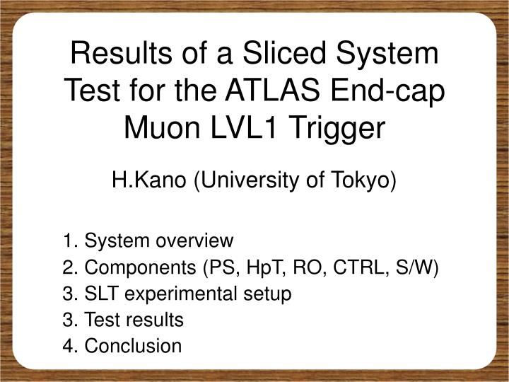
Results of a Sliced System Test for the ATLAS End-cap Muon LVL1 Trigger. H.Kano (University of Tokyo) 1. System overview 2. Components (PS, HpT, RO, CTRL, S/W) 3. SLT experimental setup 3. Test results 4. Conclusion. Introduction.

E N D
Results of a Sliced System Test for the ATLAS End-cap Muon LVL1 Trigger H.Kano (University of Tokyo) 1. System overview 2. Components (PS, HpT, RO, CTRL, S/W) 3. SLT experimental setup 3. Test results 4. Conclusion
Introduction • For the muon endcap LVL1 trigger system, full spec. custom ASICs and modules have been developed and tested. • We have completed to build these ASICs and modules. • Integration test of full components for the sliced system has been done.
Block Diagram Trigger Part MUCTPI PP G-LINK (20m) PPG50 HPT SL PS Pulse pattern generator LVDS (7m) triplet ROD doublet doublet SSW ROB ROD 3700 TGCs 320k channels Readout Part
125ns (required) 96ns PS Board & ASIC From ASD 256ch input LVDS-IN PP-ASIC PS-ASIC LVDS-OUT To H-pT
PP ASIC: 0.6mm 0.35mm 50,000gates analog + digital LVDSrx, fine-delay, and BCID function PS Board & ASIC PS ASIC: 0.35mm 250,000gates readout and L-pT trigger function
High-pT Board G-Link OUT To SL From PS LVDS IN High-pT ASIC 0.35mm BGA256 75ns (Required : TDR) 33ns
LVDS module Glink module Readout System FIFO TO CTP From SSW CPU SDRAM full func. ROD FPGA module SSW From PS TO ROD Readout System
JTAG CORE BUILDER HSC CCI Control System JTAG Using JTAG core logic generating script These JTAG cores work fine. HSC-CCI (remote VME/JTAG control system) VME1 VME2 optical cable
Run Control Conf. DB editor PP Control Software Integrated Control Software based on the ATLAS online framework i Please visit our poster
Pulse Gen. ROD SSW PS SLT Control HpT Experimental Setup SSW ROD Pulse Gen. PS HpT SL CCI bit pattern JTAG HSC SLT CTRL SL
Result of the forward wire Result (Trigger Part) Check Trigger System Hardware Test bit-pattern compare Trigger System Simulation
System Latency 1176ns < 1250ns(TDR) acceptable
Software Result (Control Part) System Configuration Run Control HSC-CCI (remote VME control system) HSC HpT Configuration by JTAG via HSC-CCI HpT Control by VME via HSC-CCI Remote VME/JTAG control : acceptable HpT CCI JTAG JTAG Operation : acceptable IC configuration by JTAG
100,000 cycles test 0 error (with 100m optical cable) Result (Readout Part) Maximum L1A trigger rate = 78kHz We can realize that … Optimized module driver, Change to high-speed CPU… for the 100kHz trigger rate.