Download
1 / 10
100 likes | 176 Views
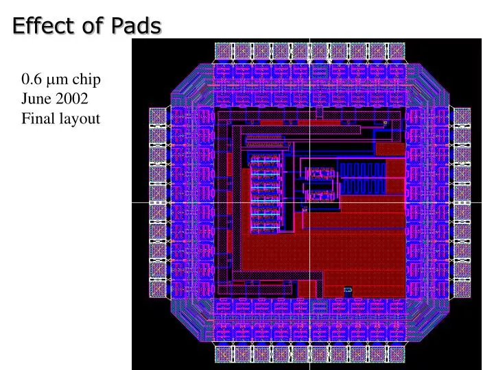
Effect of Pads. 0.6 m chip June 2002 Final layout. Effect of Pads. Left: “External” ring oscillator, 11 stages Below: Internal ring oscillator, 31 stages, output to divide-by-64 counter. Internal Osc. External Osc. One-stage delay. 112 MHz (31-stage)

E N D
Effect of Pads 0.6 m chip June 2002 Final layout
Effect of Pads Left: “External” ring oscillator, 11 stages Below: Internal ring oscillator, 31 stages, output to divide-by-64 counter
Internal Osc. External Osc. One-stage delay 112 MHz (31-stage) (equivalent to 1.16 GHz for 3 stages) 398 KHz (11-stage) (equivalent to 1.46 MHz for 3 stages) ~330 ps for internal, ~330 ns for external devices Effect of Pads: Results Summary 0.6 m chip, measurements taken by Tektronix oscilloscope with 1 pF-capacitance active probe on the breadboard Expecting similar results on a PCB with the active probe Speed ratio: 794.5 Load ratio: ~1000
Sidebar: Breadboard Capacitance Using a single inverter in 1.6 micron technology, put different extra load capacitances between the output of the inverter and ground Measured rise/fall/delay times and graphed vs. load cap. Extrapolated to where load would be zero. Vout Vin Cextra Cbboard Results: • The load capacitance of the bonding pad+bonding wire+pin+breadboard+active probe ensemble is about 15 pF. • The probe is claimed to have 1 pF load. • For the pad itself, Cadence extracts a capacitance of 0.24 pF, without the capacitances of the quite large ESD protection transistors. • A minimum-size inverter has an input capacitance of the order of 20 fF.
Chip-to-chip communication between different chips with vertical vias that require 12m x 12m metal pads Cadence-extracted capacitance 9.23 fF: Same order of magnitude as inverter load cap Unknown: Extra effects of the vertical via column to be investigated 3-D Connections in2 out2 out1 in1
3-D Connections: “Symmetric” Chip New chip submitted with structures that can be connected in 3D
3-D Connections: “Symmetric” Chip Same 31-stage planar ring oscillator with counter output Also 31-stage 3-D ring oscillator with counter output The proper pairs of pads have to be connected to each other through vertical through-chip vias post-fabrication for the circle to close. Simulation results: Planar: 142 MHz 3-D, six “layer”s: 122 MHz To counter input
3-D Connections: “Symmetric” ChipOther Structures “External” ring oscillator: Bonding pads as only loads
3-D Connections: “Symmetric” ChipOther Structures • 3-D buffer • 3-D 2-bit counter • XOR gate with output buffer • Phase delay measurement tests • 100 x minimum size NMOS for gate current measurements
3-D Connections: “Symmetric” ChipOther Structures • XOR gate with output buffer • Phase delay measurement tests