Download
1 / 18
190 likes | 379 Views
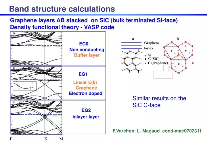
EG1. Linear E(k) Graphene Electron doped. EG2. bilayer layer. Band structure calculations. Graphene layers AB stacked on SiC (bulk terminated Si-face) Density functional theory - VASP code. EG0. Non conducting Buffer layer. Similar results on the SiC C-face.

E N D
EG1 Linear E(k) Graphene Electron doped EG2 bilayer layer Band structure calculations Graphene layers AB stacked on SiC (bulk terminated Si-face) Density functional theory - VASP code EG0 Non conducting Buffer layer Similar results on the SiC C-face F.Varchon, L. Magaud cond-mat/0702311
Graphene layers grow over the SiC surface steps T. Seyller et al. , Surface Science 600, 3906 (2006).
1 nm STM image of the first graphene layer N doped (1018 cm-3) 6H-SiC(0001) substrate from Cree Research Graphitization in ultra-high vacuum (LEED + Auger)STM experiments at room temperature and 45K 1ML graphene P. Mallet and J.Y. Veuillen, cond-mat/0702406
Well ordered layers: Graphene on SiC C-face Surface X-ray scattering - reflectivity J. Hass, E. Conrad et al. cond-mat/0702540 0th layer = buffer graphene-substrate bond << the van der Waals distance not conducting (STM, ab initio calculation, photoemission) Smooth layers, atomically flat RMS roughness (over 2µm) sG <±0.005nm Long structural coherence length Lc>300 nm Layers are not AB stacked graphite graphene layer spacing d is not graphitic (d=0.337 nm nearly turbostratic). Orientational disorder of the layers preferential orientations equal areas of rotated and non-rotated domains. mixture of stacking. Graphene growths over SiC-steps (carpet-like) (from STM)
dependence of Landau levels c =1.03 106 m/s ns≤4 1010 cm-2 EF <15 meV - sharp Dirac cone Not graphite 5-7 layers B=1.5T 1.0 0.8 1.4T 9-10 layers 1.0 0.8 Transmission 1.5T 50 layers 1.0 0.8 1.5T 1.0 0.8 HOPG ~ m m 100 200 300 400 500 600 700 Landau level spectroscopy Relative transmission EF (B) line Transition energy (meV) Wavenumber (cm)-1 M.Sadowski et al., PRL 97, 266405 (2006);cond-mat /0704.0585
K' E E K k k K’ E. McCann et al. PRL 97, 146805 (2006) : Intervalley scattering time : Warping-induced relaxation time Pseudospin, chirality 2 equivalent sublattices A and B 2 inequivalent cones at K and K’ K Intravalley scattering: no back-scattering --> Weak anti-localization (note: long-range scattering preserves AB symmetry) Intervalley scattering: back-scattering --> Weak localization (note: warping, point defects break AB symmetry locally ) DR B (T) Phase coherence time
Weak antilocalization Graphene on C-face 1.4K 50K 100 µmx1000 µm R=137 W ns=4.6 1012cm-2 µ=11600 cm2/Vs 50K 1.4K Weak antilocalization Weak localization tiv=1ps ; tw=0.28ps ; t=0.26ps Weak anti-localization observed, in agreement with Dirac particle theory Long-range scatterers dominate (remote ions in substrate) Dephasing : e- e-scattering tee~C/T C=20ps.K X.Wu et al. PRL98, 136810 (2007)
Landau plot Landau index (n) 3.8 1012 cm-2 1/B(T -1) Shubnikov de Haas oscillations wide Hall bar Small SdH amplitude in wide samples 0.1 DR/R (%) 100 µmx1000 µm 0 R= 141 /sq µ = 12000 cm2/Vs -0.1 Field (T) Landau level spacing Resistance (Ω) B(T) Anomalous Berry’s phase
1µm x 6.5µm R= 502 W/sq ns= 3.7 1012cm-2 µ= 9500 cm/Vs Shubnikov de Haas oscillations patterned Hall bar Grenoble High Magnetic Field Lab - D.Maud C.Berger et al. Phys.Stat Sol (a) in press Field (T) Rxx (Ω/sq) 1/B (T-1) 100 mK DR/R=4% DR (Ω) 1/B (T-1)
1µm x 5µm R=502 W/sq Shubnikov de Haas oscillations patterned Hall bar
Magneto-transport of a narrow patterned Hall bar Width=500 nm DR/R=10% 15 10 Landau index (n) 5 0 0 0.4 0.2 1/Bn (T-1) 200 R(Ω/sq) 100 0 0 2 4 6 8 Field (T) Anomalous Berry phase ns= 4 1012cm-2 EF= 2500 K vF= 106 m/s T(K) 4 6 9 15 35 58 mobility µ*=27000 cm2/Vs C.Berger et al. , Science 312, 1191 (2006)
theory experiment Landau level spacing Level thermally populated Lifshitz-Kosevich Dirac Landau levels dispersion DE Width used = 270 nm Patterned width = 500 nm Field Confinement : D. Mayou (2005) unpublished N. Peres et al. , Phys. Rev. B 73, 241403 (2006) C.Berger et al. , Science 312, 1191 (2006)
0.5µm x 5µm Long phase coherence length Quasi 1d ribbon T(K) 4 6 9 15 35 58 Quantum Interference effects Phase coherence length determined from weak localization and UCF : l=1.2 µm (4 K) Elastic mean free path ; boundary limited At higher temperatures l(T)~ T-2/3: e-e interactions cause dephasing.
Conductance fluctuations 0.2µm x 1µm R=208 W/sq Fluctuations reproducible invariant by reversing field and inverting I-V contacts Width of CF ≈ width of weak localization peak Amplitude ≈ e2/h Long coherence length 1080 2e2/h 1060 4K 90K R(W) 1040 1020 1000 0 2 4 6 8 B(T)
Conductance fluctuations Fluctuations reproducible invariant by reversing field and inverting I-V contacts, Width of UCF ≈ width of weak localization peak, Amplitude ≈ 0.8 e2/h 4K 0.5µmx5µm R=106 W/sq
T=250K 2 Mobility (m2/ Vs) 1 0.1 1 10 100 Width (µm) 1500 R(Ω) 10 0.1 1 100 1400 0 300 T(K) High mobility µ=10000-20000 cm2/Vs at room temperature mobility as a function of width 5 T=4 K Mobility (m2/ Vs) 3 1 Width (µm) Reduced width : - Enhanced back-scattering at ribbon edges - reduced back-scattering in quasi-1D no back-scattering due to anomalous Berry’s phase; (Note that nanotubes are ballistic conductors). T. Ando J. Phys. Soc. Jpn, 67, 2857 (1998) W.de Heer et al., cond-mat /0704.0285
Epitaxial graphene grown on SiC Highly ordered and well-defined material (structural order and smooth layers on C-face) Transport layer protected (insulating buffer layer beneath - non charged layers above) Layers above are not graphite on C-face (orientational disorder / stacking faults) Graphene properties : Dirac - chiral electrons SdH : 1 frequency only, same carrier density as photoemission Anomalous Berry’s phase Weak anti-localization (long-range scattering) Landau level spectrum Long electronic phase coherence length Ballistic properties, high mobility Weak T-dependence Anomalous transport : no quantum Hall effect Small Shubnikov-de Haas oscillations, size dependent periodic and fractal-like spectrum for high mobility samples Electrostatic potentials cannot confine Dirac electrons.
Walt de Heer, Phillip First, Edward Conrad, Alexei Marchenkov, Mei-Yin Chou Xiaosong Wu, Zhimin Song, Xuebin Li, Michael Sprinkle, Nate Brown, Rui Feng, Joanna Haas, Tianbo Li, Greg Rutter, Nikkhil Sarma School of Physics - GATECH, Atlanta Thomas Orlando, Lan Sun, Kristin Thomson School of Chemistry - GATECH, Atlanta Jim Meindl, Raghuna Murali, Farhana Zaman Electrical Engineering - GATECH, Atlanta Gérard Martinez, Marcin Sadowski, Marek Potemski, Duncan Maud, Clément Faugeras CNRS - LCMI, Grenoble Didier Mayou, Laurence Magaud, François Varchon, Cécile Naud, Laurent Lévy, Pierre Mallet, Jean-Yves Veuillen, Vincent Bouchiat CNRS - Institut Néel, Grenoble Patrick Soukiassian, CEA - Saclay Jakub Kiedzerski, MIT-Lincoln Lab Joe Stroscio, Jason Crain, NIST Ted Norris, Michigan University Alessandra Lanzara, University Berkeley