Download
1 / 47
480 likes | 1.04k Views
CE AMPLIFIERS. CE AMPLIFIERS. The first step is to set up an operating or ‘Q’ point using a suitable bias circuit. We will, by way of introduction, use a so called load line technique to see the interplay between the circuit and device constraints on voltage and current.

E N D
CE AMPLIFIERS • The first step is to set up an operating or ‘Q’ point using a suitable bias circuit. • We will, by way of introduction, use a so called load line technique to see the interplay between the circuit and device constraints on voltage and current. • This will provide a graphical analysis of amplifier behaviour.
CE AMPLIFIERS • The following (simple) bias circuit uses a single resistor RB to fix the base current. • It is not very good since the emitter/collector currents and hence the operating point (IC, VCE) vary with β. • This will be improved with stabilised bias circuits in due course.
CE AMPLIFIER, Simple bias +VCC IC IB RB RC GND
CE AMPLIFIER, Simple bias +VCC IC IB RB RC VCE VBE GND
CE AMPLIFIER, Simple bias • To enable us to look at a particular numerical example we choose the supply voltage VCC = 5V and RC = 2.5 kΩ
CE AMPLIFIER, Simple bias +5 IC RB 2.5 x 10³ GND
CE AMPLIFIER, Simple bias • In later discussions an a.c. signal (and an additional load resistor) will be coupled to the d.c. circuit using coupling capacitors. • The capacitor values are chosen so that their impedance (1/ C) is negligibly small (zero) at the a.c.(signal) frequency (or over the operating frequency range). • A capacitor acts as a short circuit for d.c. and the d.c. bias circuit can be designed independently of the a.c. source and any ‘a.c. load’.
CE AMPLIFIER, Simple bias +5 IC RB 2.5 x 10³ GND
+VCC IC RC VCE GND CE AMPLIFIER, Simple bias From Kirchhoff, for the output,
CE AMPLIFIER, Simple bias • Numerically, 5 - 2.5 x 10³ IC-VCE =0 • Or, rearranging, IC = (5 – VCE )/ (2.5 x 10³) • A plot of IC against VCE is a straight line with slope (– 1/ 2.5 x 10³) • It is called a load line and represents the variation of IC with VCEimposed by the circuit or load.
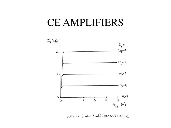
CE AMPLIFIER, Simple bias • Another variation of IC with VCE is determined by the output characteristic.
CE AMPLIFIER, Simple bias • Another variation of IC with VCE is determined by the output characteristic. • The two relationships can be solved graphically for IC and VCE.
Thus we calculate three points on the load line IC = (5 – VCE )/ (2.5 x 10³) as IC =0, VCE =5V IC = 1mA, VCE =2.5V VCE =0V, IC =5/2500 A = 2mA. To enable us to plot it on the output characteristic. CE AMPLIFIER, Simple bias
CE AMPLIFIER, Simple bias • The region along the load line includes all points between saturation and cut-off. • The base current IB should be chosen to maximise the output voltage swing in the linear region. • Bearing in mind that VCE (Sat) 0.2 V and VCE Max = 5V choose the operating (Q) point at IB = 10 μA.
CE AMPLIFIER, Simple bias ‘Operating’ or Q point set by d.c. bias.
+VCC IB RB VBE GND CE AMPLIFIER, Simple bias • From Kirchhoff, for the input,
CE AMPLIFIER, Simple bias • Remembering that VBE ~ 0.6 V (the base or input characteristic is that of a forward biased diode) we can find RB ~ 440 kΩ.
CE AMPLIFIER, Simple bias • A a.c. signal is superimposed on top of the d.c. bias level. • We are interested in the voltage and current gains for this a.c. component.
VCC IC RL RB VCE RS VS GND CE AMPLIFIER RC Signal input Signal output
CE AMPLIFIER • The Q (d.c. bias) value of VCE is about 2.5 V • The maximum positive signal swing allowed is, therefore (5-2.5) V = 2.5 V (The total • The maximum negative voltage swing allowed is (2.5 –0.2) V =2.3 V • The maximum symmetric symmetric signal swing about the Q point is determined by the smaller of these, i.e. it is 2.3 V.
CE Amplifier • To find the voltage and current gains using the load line method we must use the input and output characteristics.
CE Amplifier Diode dynamic resistance for signals = 1/slope at Q point! Defines transistor input impedance for signals Remember we selected IB = 10 μA
CE Amplifier • From the input curve we estimate that as IB changes by 5μA about the bias level of 10μA then the corresponding change in VBE is about 0.025 V. • When iB =5μA, vBE = 0.5875V; when iB =15μA, vBE = 0.6125.
CE Amplifier • From the output characteristic curve we move up and down the load line to estimate that as IB changes by 5μA the corresponding change in VCE is about –2.5 V. (Note the negative sign!) • When iB =5μA, vCE = 3.75V; when iB =15μA, vCE = 1.25V
CE Amplifier • From the input curve we estimate that as IB changes by 5μA about the bias level of 10μA then the corresponding change in VBE is about 0.025 V. • When iB =5μA, vBE = 0.5875V; when iB =15μA, vBE = 0.6125.
CE AMPLIFIER ‘Operating’ or Q point set by d.c. bias.
CE Amplifier • The CE small signal (a.c.) voltage gain is
CE Amplifier • From the output characteristic curve we also see that as we move up and down the load line a change in IB of 5μA produces a corresponding change in IC of 5mA. • The a.c. signal current gain is 100. • This is consistent with the ideal characteristic uniform line spacing, i.e. β = 100 = constant.
CE AMPLIFIER ‘Operating’ or Q point set by d.c. bias.
Ideal CE Amplifier Summary • The CE voltage and current gains are high • The voltage gain is negative, i.e. the output signal is inverted. • The d.c. bias current sets the signal input impedance of the transistor through the dynamic resistance. • IC = β IB ; iC = β iB.
Ideal CE Amplifier Summary • Two of these statements: • The d.c. bias current sets the signal input impedance of the transistor through the dynamic resistance. • IC = β IB ; iC = β iB. will be used to derive our simplified small signal equivalent circuit of the BJT. (It is simplified because it is based on ideal BJTs)
vout vin RL GND Additional a.c. Load • Suppose an a.c. coupled load RL = 2.5 kΩ is added VCC RC C
Additional a.c. Load • The ‘battery’ supplying the d.c. supply VCC has negligible impedance compared to the other resistors, in particular RC. • It therefore presents an effective ‘short-circuit’ for a.c. signals. • The effective a.c. load is the parallel combination of RC and RL . (From the collector C we can go through RC or RL to ground)
Additional a.c. load a.c. short via d.c. supply RC iC RL GND
Additional a.c. load iC RL RC vce GND
Additional a.c. Load • We now need to construct an a.c. load line on the output characteristic. • This goes through the operating point Q and has slope • This is hard to draw!
Additional a.c. Load a.c. load line, drawn with required slope through Q point.
Additional a.c. Load • The available voltage swing and the voltage gain are calculated using the a.c. loadline. • Symmetric swing reduced to about 1.25 V • Voltage gain reduced to about –50.
Stabilised Bias Circuits • These seek to fix the emitter current independently of BJT parameter variations, principally in β. • This is best achieved by introducing an emitter resistance and setting the base voltage via a resistor network (R1, R2) which acts as a potential divider (provided IB can be assumed small)
VCC RC R1 vout RS R2 RE VS GND Stabilised Bias Circuit Bias bit of the circuit, a.c. source and load capacitor coupled. RE is capacitor by-passed (shorted) for a.c. signals
Stabilised Bias Circuit • See handout for a detailed analysis of this bias circuit • We will also look at a worked example of a transistor amplifier based on such a stabilised bias circuit once we have established an a.c. equivalent circuit for the transistor.
Stabilised Bias Circuit • Finally we give another circuit which provides bias stability using negative feedback from the collector voltage. +VCC RC RB IC D.C collector voltage VC IB VBE =0.6 V GND
Stabilised Bias Circuit +VCC IRC RC RB IC D.C collector voltage VC IB VBE =0.6 V GND
Stabilised Bias Circuit +VCC IRC RC RB IC D.C collector voltage VC IB VBE =0.6 V GND
For example, increasing , increases IC which lowers the collector voltage VC and hence and IB andIC Stabilised Bias Circuit +VCC RC RB IC D.C collector voltage VC IB VBE =0.6 V GND