Download
1 / 58
580 likes | 586 Views
RD42 Status Report. Development of CVD Diamond Tracking Detectors for Experiments at High Luminosity Colliders presented by P. Weilhammer University of Perugia/CERN For the RD42 COLLABORATION. RD42 Collaboration: 24 institutes for development of CVD diamond detectors.

E N D
RD42 Status Report Development of CVD Diamond Tracking Detectors for Experiments at High Luminosity Colliders presented by P. Weilhammer University of Perugia/CERN For the RD42 COLLABORATION RD42 Status Report 15.02.2006
RD42 Collaboration: 24 institutes for development of CVD diamond detectors • http://rd42.web.cern.ch/rd42/ • Industrial Partner: • Element Six Ltd • H. Murphy, D. Twitchen, A. Whitehead (Element Six, UK) RD42 Status Report 15.02.2006
RD42 Collaboration: Institutes from HEP, Heavy Ion Physics, Hadron Therapy Centers and Solid State Physics RD42 Status Report 15.02.2006
Still growing – new groups joined RD42 during last 18 months: DESY Zeuthen St. Petersburg Fachhochschule fuer Wirtschaft und Technik-Vienna ITEP Moscow Josef Stefan Institute Ljubljana RD42 Status Report 15.02.2006
What are the radiation environments to be expected after initial LHC running: From M. Moll Pixel2005 Bonn Scenario for 5 years running SLHC RD42 Status Report 15.02.2006
Radiation Hardening of Silicon Detectors: • Main adverse effects after irradiation: (M. Moll, Pixel2005, Bonn) • Change ofeffective doping concentration (higher depletion voltage, under- depletion) • Increase ofleakage current(increase of shot noise, thermal runaway) • Increase of charge carrier trapping (loss of charge) RD42 Status Report 15.02.2006
Remedies for Silicon: Material engineering Device engineering Change of detector operational conditions Maybe new materials: 4H-SiC, 6H-SiC, GaN, GaAs, CZT, a-Si(H), ….CVD Diamond However to get enough charge after irradiation, avoid extreme leakage currents and not to have the signal dominated by noise: quite extreme running conditions required ( in Silicon case): Low temperatures, very high bias voltages,……. RD42 Status Report 15.02.2006
In this situation it is a challenge to continue studies of CVD diamond as a detector material; in particular for application in environments with the highest integrated radiation fluxes RD42 Status Report 15.02.2006
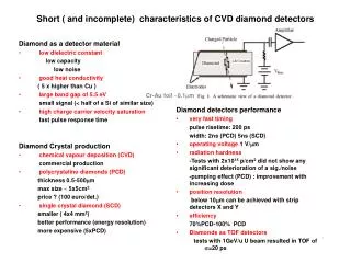
Important Properties of CVD diamond for Tracking: • GOOD • Both electron and hole mobilities are high, signal collection fast • At E = 1 V/m Diamond= 1.67 x 107 cm/sec • Silicon = 3.8 0 x 106 cm/sec • Load capacitances of sensor 2.1 times lower than for Si ( lower epsilon) because of low e. • Diamond has 1.3 times less radiation length compared with Si • “Good” CVD Diamond is an insulator ( high band gap) with resistivity greater than 1014 Wcm. • Leakage current: Ileak ~ 100 pA/cm2 for a 500m thick sample. • Low load capacitances are limiting electronic noise RD42 Status Report 15.02.2006
NOT SO GOOD, but maybe compensated by good properties The generated charge in diamond is 3600 electron- hole pairs per 100 m compared with 10600 electron hole pairs in Si. Slightly more favorable when one compares generated charge per .3% of radiation length: Diamond: ~13900 mean charges in 361 m Silicon: ~26800 mean charges in 282 m Lifetime of both holes and electrons is smaller than the transit time (now comparable to) at 1V/mm ( in un-irradiated silicon lifetime is 10’s of ms): signal loss in bulk by trapping RD42 Status Report 15.02.2006
Development of CVD Diamond Radiation Sensors: RD42 Collaboration: • AN OVERVIEW AND SOME RECENT RESULTS • Content of this presentation: • POLYCRYSTALLINE CVD DIAMOND (pCVD) • Charge Collection, Results from Irradiations, the ATLAS Pixel Module, Beam diagnostics and Monitoring with Diamonds • 2. SINGLE CRYSTAL CVD DIAMONDS (sCVD) • Charge Collection, Charge Carrier Properties via TCT • 3. SOME APPLICATION RD42 Status Report 15.02.2006
Charge Collection and Radiation Hardness of pCVD Diamond RD42 Status Report 15.02.2006
Principle of detector operation Growth-Side e R h Substrate-Side Electric field m and t are “effective” mobility and lifetime collected charge t d “collection distance” e= Q / Q0 collection efficiency RD42 Status Report 15.02.2006
State of the art pCVD material Photo of Sample 1.1 mm thick Growth side 20 mm 50 mm What Charge Collection Distance can one get RD42 Status Report 15.02.2006
Saturation Velocity of carriers reached at ~ .5 V/mm 90Sr Source 300mm ~11000 eh pairs mean Charge Collection Distance of such samples RD42 Status Report 15.02.2006
I-V Curve for a pCVD Sample ~ pA ~0.01 pA RD42 Status Report 15.02.2006
History of Radiation Hardness Measurements with pCVD Diamonds Sample CDS-69 had originally ~ 160mm ccd, 520 mm thick RD42 Status Report 15.02.2006
Irradiation with protons to 1.8 x 10¹⁶ p/cm2 (~500Mrad) Relative charge as function of fluence at fixed field Sample CD113: t= 490 mm, CCD = 225 mm RD42 Status Report 15.02.2006
Single Crystal CVD Diamonds Summary of results on charge collection and carrier properties RD42 Status Report 15.02.2006
Single Crystal CVD Diamond Samples • Rd 42 has research contract with Element6 to further develop this material • scCVD can be grown at present to ~ 1cm x 1 cm size, ~ 1mm thick • Biggest sample fabricated was 14 mm x 14 mm RD42 Status Report 15.02.2006
Collected charge for a scCVD sample Sample is ~435 micron thick • Single Crystal CVD collects all created charge at ~0.2 V/mm • Single crystal CVD does not “pump” RD42 Status Report 15.02.2006
Collected Charge measured on Samples in GSI Charge from integration of current pulses (see below) shows that charge collection is complete above 0.35 V/mm for both holes and electrons A w value of 12.8 eV/(eh)pair is derived from this RD42 Status Report 15.02.2006
Pulse Height Spectrum with 90Sr Source from 4 scCVD samples with different thicknesses t = 210mm t = 320mm t = 685 mm t = 435 mm RD42 Status Report 15.02.2006
Most probable charge versus thickness of samples RD42 Status Report 15.02.2006
Charge carrier properties in Single Crystals Measure charge carrier properties important for signal formation electrons and holes separately Use a-source (Am 241) to inject charge Injection Depth about 14mm compared to 470mm sample thickness Use positive or negative drift voltage to measure material parameters for electrons or holes separately Amplify ionization current a Electrons only Or Holes only V The pulse shape of the induced current is recorded (Transient Current Technique) RD42 Status Report 15.02.2006
Ionization Current in a sCVD sample • Drift time and mobility • Charge Lifetime • Internal electrical field • Transit time of charge cloud • Signal edges mark start and arrival time of drifting charge cloud • Two effects determine the shape during the drift for this sample • Charge trappingduring drift if any • Space charge : decrease of current for holes / increase for electrons with time Voltage increase tc RD42 Status Report 15.02.2006
Another Single Crystal Sample from E6 (measured in Bonn) Indicates that the electric field in this sample is uniform no space charge! Holes Electrons RD42 Status Report 15.02.2006
Six more samples from E6 measured in GSI: also uniform electric field observed; This seems to be the normal case in Element6 scCVD samples RD42 Status Report 15.02.2006
The measured drift velocity • Average drift velocity for electrons and holes • Extract low field mobility m0 and saturation velocity vs • m0 for the 2 first samples: • Electrons: 1714 cm2/Vs and 1884 cm2/Vs • Holes: 2064 cm2/Vs and 2239 cm2/Vs • Saturation velocity: • Electrons: 0.96 107 cm/s and .88 x 107cm/s • Holes: 1.41 107 cm/s and 1.33 x 107 cm/s RD42 Status Report 15.02.2006
Preliminary carrier lifetime measurements • Extract carrier lifetimes from measurement of total charge Lifetime >35ns Charge trapping doesn’t seem to limit signal lifetime -> full charge collection (for typical operation voltages and thickness) RD42 Status Report 15.02.2006
More GSI Measurements on Spectroscopy Energy resolution measured with sc CVD diamonds is close to what is achieved with silicon. RD42 Status Report 15.02.2006
A full ATLAS Pixel Module with pCVD Diamond Most of this done by the Bonn group in RD42: M. Mathes, F.Huegging, J. Weingarten, N Wermes and H. Kagan (OSU) RD42 Status Report 15.02.2006
A complete ATLAS pixel module has been assembled over the last two years Module equipped with 16 fully radhard IBM readout chips Several assembly steps RD42 Status Report 15.02.2006
Very short test in the high energy ATLAS test beam at CERN Beam profile All channels are working RD42 Status Report 15.02.2006
The ATLAS Pixel Module in a DESY Test Beam Hit map is good The edge is the trigger scintillator RD42 Status Report 15.02.2006
Noise and Threshold Plots Results: Noise ~ 137 e- ENC Mean Threshold : 1450 e- Threshold Spread ~ 25 e- RD42 Status Report 15.02.2006
Correlation with Beam Telescope and Spatial Resolution Correlation of hits in beam telescope and pixel module Residual is ~17 mm, includes multiple scattering ( low energy electrons) RD42 Status Report 15.02.2006
Efficiency is reasonably high Above 97% RD42 Status Report 15.02.2006
Beam Diagnostics and Monitoring with pCVD Diamonds RD42 Status Report 15.02.2006
Beam Diagnostics & Monitoring with Diamonds(ATLAS, CMS, CDF, Belle, BaBar) “DC current” Uses beam induced DC current to measure dose rate close to IP Benefits from very low intrinsic leakage current of diamond Can measure at very high particle rates Simple DC (or slow amplification) readout Examples: BaBar Belle CDF Single particle counting Detect min. ionizing particles Benefits from fast diamond signal Allows more sophisticated logic coincidences, timing measurements Requires fast electronics (GHz range) with very low noise Examples Atlas Beam conditions monitor • Common Goal: measure interaction rates & background levels in high radiation environment • Input to background alarm & beam abort RD42 Status Report 15.02.2006
The ATLAS Beam Conditioning Monitor (BCM) Principle and Main Goals • Instantaneous measurement of beam conditions • interaction rate • background condition • warning/alarm/abort signals • Measurement every BX • Distinguish between interaction events and otherevents RD42 Status Report 15.02.2006
Set-Up in ATLAS Detector 2 detector stations, symmetric in z, 2z0 apart TAS (collimator) event: Δt=2z0/c Interaction event: Δt = 0, 25, … ns RD42 Status Report 15.02.2006
Baseline requirements: beam abort operation • one 7 TeV proton on TAS gives ~ 1 MIP/cm2 inside PST • Installation at Δt = 12.5 ns -› Δz = 3.75 m • Rise-time < 1 ns • Pulse-width < 3 ns • Base-line restoration < 10 ns RD42 Status Report 15.02.2006
38 cm 183cm ATLAS Beam Conditions Monitor @ LHC • 4 BCM stations on each side of the Pixel detector • Mounted on Pixel support structure at z = +/- 183.8 cm and r = 7 cm • Each station: 1cm2 detector element + Front-end analog readout RD42 Status Report 15.02.2006
Requirements for luminosity determination • additional to ATLAS main luminosity monitor LUCID Single MIP sensitivity • Poisson with average of < 1 MIP per diamond detector • S/N for MIP’s ~10:1 before irradiation • 4 detectors per station (coincidence) Simulation RD42 Status Report 15.02.2006
Poly-CVD Diamonds as Sensors ATLASBCM Module • Radiation hard • Shown to withstand > 1015 p/cm2 • Fast and short signal • High charge carrier velocity • Narrow pulses partially due to short charge lifetime • Operates with a high drift field • Carrier velocity close to saturation velocity • Very Low leakage current after irradiation • Does not require detector cooling CVD Diamond RD42 Status Report 15.02.2006
Many tests already done: • beam-test measurements • evaluation of prototypes of detectors and FE electronics • Boston beam-test: May 2004 • SPS CERN beam-test: November 2004 • KEK test beam • bench-tests • Sr-90 based tests of setups • evaluation of prototypes of detector boxes with FE • evaluation of back-end electronics • QA of final detectors • different mounting possibilities • irradiations of components This one chosen RD42 Status Report 15.02.2006
Some Results • SPS H8 pion beam - MIP’s • Diamond detectors • 2 double-deckers: • CDS154+CDS155, w=360 µm • CDS159+CDS160, w=515 µm • HV Bias ~2 V/µm • Placed at 0o and 45o • 2 scintillators for triggering • LeCroy 1 GHz scope A(V) ~5mV typical event <2ns t(ns) RD42 Status Report 15.02.2006