Download
1 / 42
420 likes | 434 Views
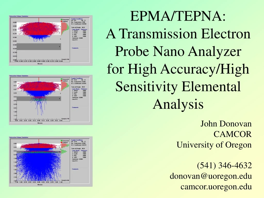
EPMA/TEPNA: A Transmission Electron Probe Nano Analyzer for High Accuracy/High Sensitivity Elemental Analysis. John Donovan CAMCOR University of Oregon. (541) 346-4632 donovan@uoregon.edu camcor.uoregon.edu. CAMCOR Center for Advanced Materials Characterization in ORegon.

E N D
EPMA/TEPNA: A Transmission Electron Probe Nano Analyzerfor High Accuracy/High Sensitivity Elemental Analysis John Donovan CAMCOR University of Oregon (541) 346-4632 donovan@uoregon.edu camcor.uoregon.edu
CAMCORCenter for Advanced Materials Characterization in ORegon • Nano Fabrication Facility- SEM lithography, Helios DBFIB • Kurt Langworthy, klangwor@gladstone.uoregon.edu • Surface Analytical Laboratory- XPS, Auger, SIMS (TOF) • Steve Golledge, golledge@darkwing.uoregon.edu • X-ray Diffraction- XRD (powder, grazing incidence, single crystal) • Lev Zahkarov, lev@darkwing.uoregon.edu • High Resolution- Titan, Technai TEMs • Joshua Razink, jrazink@uoregon.edu
UofO CAMCOR MicroAnalytical Facility • Cameca SX50 EPMA • Cameca SX100 EPMA • FEI Quanta VP-ESEM SEM
An SEM with EDS! What is elemental characterization for most material scientists?
Electron Probe Micro Analysis (EPMA) • What Makes a Microprobe? • High Stability Electron Source • Reflected Light Optics • Focussing WDS X-ray Optics • Standards Because there is no such thing as “standardless” WDS. NIST to EDS community: Don’t press the “button”!
Error Distribution for a Commercial Standardless EDS Analysis: 1995 Error bins are 5% wide 95% range =+25% rel Newbury, D. E., Swyt, C. R., and Myklebust, R. L., "'Standardless' Quantitative Electron Probe Microanalysis with Energy-Dispersive X-ray Spectrometry: Is It Worth the Risk?", Analytical Chemistry, 67 (1995) 1866-1871.
Standardless Analysis: Is it any better in 2011? FeS (meteoritic troilite) Spectrum: Acquisition FeS troilite (STD MT C) El AN Series unn. C norm. C Atom. C Error Relative Error % [wt.%] [wt.%] [at.%] [ wt.%] (C norm) -------------------------------------------- Fe 26 K-ser 62.40 62.86 49.29 1.7 -1.1% S 16 K-ser 36.86 37.14 50.71 1.3 +1.8% -------------------------------------------- Total: 99.26 100.00 100.00 Analysis of Binary Sulfides with a commercial “standardless” analysis protocol. Apparent formula: FeS
Standardless Analysis: Is it any better in 2011? FeS (meteoritic troilite) Spectrum: Acquisition FeS troilite (STD MT C) El AN Series unn. C norm. C Atom. C Error Relative Error % [wt.%] [wt.%] [at.%] [ wt.%] (C norm) -------------------------------------------- Fe 26 K-ser 62.40 62.86 49.29 1.7 -1.1% S 16 K-ser 36.86 37.14 50.71 1.3 +1.8% -------------------------------------------- Total: 99.26 100.00 100.00 ZnS Spectrum: Acquisition (ZnS (STD MT C) El AN Series unn. C norm. C Atom. C Error Relative Error % [wt.%] [wt.%] [at.%] [wt.%] (C norm) --------------------------------------------- Zn 30 K-ser 67.94 76.15 61.02 1.9 +14% S 16 K-ser 21.28 23.85 38.98 0.8 -28% --------------------------------------------- Total: 89.23 100.00 100.00 CuS Spectrum: Acquisition El AN Series unn. C norm. C Atom. C Error Relative Error % [wt.%] [wt.%] [at.%] [wt.%] (C norm) --------------------------------------------- Cu 29 K-ser 69.02 76.43 62.07 1.9 +15% S 16 K-ser 21.29 23.57 37.93 0.8 -30% --------------------------------------------- Total: 90.31 100.00 100.00 Analysis of Binary Sulfides with a commercial “standardless” analysis protocol. And this is analysis with energetic K-shell peaks! This is only one snapshot of the 2011 performance of one system. A more complete study is underway. Apparent formula: FeS Apparent formula: Zn3S2 From Newbury, M&M 2011 Apparent formula: Cu3S2
Accuracy of EDS/WDS with Standards 95% range is +/- 8% for a “worst case” database
Donovan, et. al., 2011, Amer. Min. That other thing... sensitivity!
Is that my signal? ~50 nm Fe, Nb, Se film on Si wafer (20 keV, 30 nA) Thin films are a trace element problem... Nope… Si sum peak!
Nb peak not identified as all Si “sum peak” identified as Sn No Th in sample! Dale Newbury’s infamously described ID “blunders” are still here… Fe, Nb, Se thin film on Si
WO3 nano-particles on Si Si sum peak is not 3 sigma, but neither are the W peaks! Like thin films, nano-particles also present a sensitivity problem...
NIST SDD (4 quads) 170 ppm 5 Spectrometers 1 ppm (normal PET crystal)
WDS Spectrometers An electron microprobe generally has 3-5 spectrometers, with 1-4 crystals in each. Here with its cover off. Crystals (2 pairs) Proportional Counting Tube (note tubing for gas) PreAmp
Not a problem for nano films and particles… or polished mounts. Allows quantitative analysis of Be, B, C, N, O, F, etc Bragg Spectrometers and “defocussing”
Beam Penetration • Beam penetration decreases with Z • Beam penetration increases with energy • Electron range ~ inelastic processes • Electron scattering (aspect) ~ elastic processes
What is a Thin Film (for EPMA)? • Films greater than 5-10 um can be considered “infinitely thick” • Normal EPMA • Films between 5000-500 angstroms are “normal” • Use multi-voltage analysis (MVA) and model geometry • Films less than 500 angstroms are “ultra-thin” • Use MVA (and take special precautions: surface contamination, plasma cleaning prior to analysis)
(a) Schematic of Thin Film Calculations (b) Figure 4 - Flow charts of the iteration methods used (a) when no element with an unknown concentration is present in several layers; (b) when such an element is present in several layers. From Thiot
Thick (Bulk) Analysis of SRM 2135C(Ni-Cr multi-layer on Si)What if we “neglect” geometry? Results in weight % Every electron energy gives a different (and wrong) result! (even if we do not include Si in the ratio calculation)
NIST Thin Film Standard SRM 2135c Thin Film (traverse 1)- homogeneous model (all elements in one layer on Si) 15, 20 25 keV
2:1 attempted ratio Simple Film on Substrate Example Johnson Lab (UofO)
1:1:1:1 attempted ratio Insulating Substrate (carbon coated) Keszler Lab (OSU)
1:1:1 attempted ratio Complex substrate (Corning 1737 glass) Keszler Lab (OSU)
Nominal Thickness Multiple Substrates Keszler Lab (OSU)
Fixed Thickness (from XRR) Duplicate Elements Johnson Lab (UofO) Phung, et. a l., "Determination of the Composition Ultra Thin Ni-Si Films" (X-ray Spectrometry, 2008)
Thin Film Quantification • A variety of substrates can be measured with accuracy approaching normal “thick” samples • Thickness can also be calculated, given density and provided that the element is not in the film and substrate, or can be confined by stoichiometry. • Samples with multiple substrates can be analyzed quantitatively. • X-ray diffraction data used in conjunction with EPMA allows composition to be calculated for “duplicate” elements (in both film and substrate).
A proposal for a TEPNA instrument... The proposed Electron Probe Nano Analyzer integrates several new detection technologies to optimize compositional characterization with a target spatial resolution of ~10 nm for “as deposited” films and particles in the range of tens to hundreds of nanometers in thickness, while still attached to electron opaque substrates.
100 nm thick, 0.01 um dia. Requires a 1000 fold improvement in sensitivity! (1,000,000 x fewer atoms but 1000 x thicker film) EPMA WDS Monolayer Detection Demonstrated... 0.1 nm thick, 10 um dia. The increase in signal as a 10 mm diameter beam is scanned over a region containing a monolayer of Hf atoms deposited on a Si substrate using a Cameca SX50
Utilizing high energy emission lines with higher fluorescent yields • e.g., Nb La = 3.5%, Nb Ka = 74% (20-30 fold improvement) How do we improve sensitivity 1000 fold? • Energy filtering of Be exit windows for high energy emission lines (?) • Why not do it now? Goldstein et. al. 1992
Highest effective fluorescent yields are found for element emission lines whose absorption edges are higher than 8 keV Zn Ka is 9.659 keV Nb Ka is 16.58 keV In 2 cm of Ar 37% of Zn Ka trans. 86% of Nb Ka trans. In 2 cm of Xe .05% of Zn Ka trans. 59% of Nb Ka trans. While still retaining soft x-ray sensitivity!
Reduced continuum signal using “faraday cup” TEM grid holders • - preliminary measurements show a 30% reduction in continuum Other sensitivity improvements are possible... • High geometric efficiency using small FC or large area crystals • - 3 to 4 fold improvement • Multiple WDS spectrometers in “aggregate” mode • - 2 to 5 fold improvement using only software • Increased counting time/beam current in electron “transmission mode” • - 30 keV beam through 100 nm of FeS2 loses ~30 eV of energy • - assume 2 to 5 fold improvement by increasing time/current
Transmission Electron Probe Nano Analyzer (TEPNA) An electron beam instrument that integrates several innovations to optimize compositional characterization with a target spatial resolution of ~20 nm for samples in the range of tens to hundreds of nanometers in thickness on various electron opaque substrates. The proposed TEPNA complements existing analytical techniques by providing an unmet need for quantitative compositional analysis conveniently intermediate between that currently achieved by wavelength dispersive x-ray (WDX) electron probe micro analysis (EPMA) and energy dispersive x-ray (EDX) analytical electron microscopy (AEM).
Current/Future Capabilities of EPMA WDS: Bulk Analysis: single digit PPM sensitivity (and accuracy) - even for light elements, pathological overlaps Thin Film/Particle Analysis: available now for major/minor elements - high accuracy (~2-3%), high sensitivity (2-10 PPM) - with typical ~1 um beam diameters TEPNA: Transmission Electron Probe Nano Analyzer - requires 1000 fold sensitivity improvements for 20 nm beam - utilize high energy, 30 keV, 20 nm electron beam - high fluorescent yield lines (> 8 keV) - tandem gas flow/SDD photon counters (full energy sensitivity) - large area/small FC crystals/spectrometers - aggregate intensities in software
Contact Information: John Donovan Micro Analytical Facility CAMCOR University of Oregon Eugene, OR (541) 346-4632 Email: donovan@uoregon.edu Web: camcor.uoregon.edu