Download
1 / 18
180 likes | 182 Views
This lecture revisits the CMOS inverter and explores the complementary nature of CMOS logic circuits. It introduces CMOS NAND and NOR gates and discusses the effective resistance and capacitance for CMOS logic transitions. The lecture also covers the model for MOS transistors involved in CMOS digital computation.

E N D
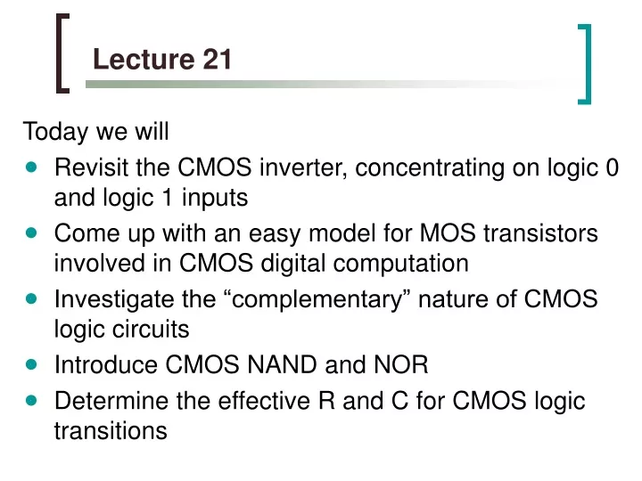
Lecture 21 Today we will • Revisit the CMOS inverter, concentrating on logic 0 and logic 1 inputs • Come up with an easy model for MOS transistors involved in CMOS digital computation • Investigate the “complementary” nature of CMOS logic circuits • Introduce CMOS NAND and NOR • Determine the effective R and C for CMOS logic transitions
CMOS Inverter VDD (Logic 1) VGS(n) = VIN VGS(p) = VIN – VDD VDS(n) = VOUT + VGS(p) - S VOUT D + VDS(n) _ D VIN + VGS(n) - S
CMOS Analysis ID(n) As VIN goes up, VGS(n) gets bigger and VGS(p) gets less negative. NMOS I-V curve PMOS I-V curve (written in terms of NMOS variables) NMOS cutoff (open circuit) PMOS triode (with VDS(p) = 0 V) VIN < VTH(n) (e.g., logic 0) VDS(n) (=VOUT) VDD
CMOS Analysis ID(n) NMOS I-V curve PMOS I-V curve (written in terms of NMOS variables) VIN > VDD + VTH(p) (e.g., logic 1) PMOS cutoff (open circuit) NMOS triode (with VDS(n) = 0 V) VDS(n) (=VOUT) VDD
D G S Model for Digital Computation • This leads us to a simpler model for transistors in CMOS circuits, when VIN is fully logic 0 or logic 1. VGS = VDD (for NMOS) VGS = -VDD (for PMOS) VGS = 0 V D G S Transistor is not cutoff, but zero current flow of partner transistor causes VDS = 0 V. Transistor is cutoff. Zero current flow.
Practice • Use this model to find VOUT for the circuits below. VDD VDD VOUT VIN = 0 V VOUT VIN = VDD
CMOS NAND VDD S S A PMOS1 PMOS2 AB B NMOS1 S NMOS2 S
More Practice Verify the logical operation of the CMOS NAND circuit: VDD VDD S S S S A = 0V A = 0V B = 0V B = VDD S S S S
More Practice Verify the logical operation of the CMOS NAND circuit: VDD VDD S S S S A = VDD A = VDD B = 0V B = VDD S S S S
CMOS Networks • Notice that VOUT gets connected to either VDD or ground by “active” (not cutoff) transistors. • We say that these active transistors are “pulling up” or “pulling down” the output. • NMOS transistors = pull-down network • PMOS transistors = pull-up network • These networks had better be complementary or VOUT could be “floating”—or attached to both VDD and ground at the same time.
VDD CMOS NOR VDD S A S S A S B B S S S S CMOS NAND vs. NOR CMOS NAND AB A+B
Complementary Networks • If inputs A and B are connected to parallel NMOS, A and B must be connected to series PMOS. • The reverse is also true. • Determining the logic function from CMOS circuit is not hard: • Look at the NMOS half. It will tell you when the output is logic zero. • Parallel transistors: “like or” • Series transistors: “like and”
metal metal + - Resistance and Capacitance VGS > VTH(n) gate • The separation of charge by the oxide insulator creates a natural capacitance in the transistor from gate to source. • The silicon through which ID flows has a natural resistance. • There are other sources of capacitance and resistance too. drain metal oxide insulator _ _ _ _ n-type e e e n-type e e + + + _ + + + _ _ _ _ p-type h h h h h h h h h h metal
VDD S VOUT1 VDD D e e S D VOUT2 D D S S Gate Delay—The Full Picture • Suppose VIN abruptly changed from logic 0 to logic 1. • VOUT1 may not change quickly, since is attached to the gates of the next inverter. • These gates must collect/discharge electrons to change voltage. • Each gate attached to the output contributes a capacitance. VIN
VDD S VOUT1 VDD D e e S D VOUT2 D D S S Gate Delay—The Full Picture • Where will these electrons come from/go to? • No charges can pass through the cutoff transistor. • Charges will go through the pull-down/pull-up transistors to ground. These transistors contribute resistance. VIN
VDD S VOUT1 VDD D S D VOUT2 D D S S Computing Gate Delay 1. Determine the capacitance of each gate attached to the output. These combine in parallel. Higher fan-out = more capacitance. 2. Determine which transistors are pulling-up or pulling-down the output. Each contributes a resistance, and may need to be combined in series and/or parallel. 3. The C from 1) and R from 2) are the RC for the VOUT1 transition. VIN tp = (ln 2)RC
Example • Suppose we have the following circuit: • If A and B both transition from logic 1 to logic 0 at t = 0, find the voltage at the NAND output, VOUT(t), for t ≥ 0. Logic 0 = 0 V Logic 1 = 1 V NMOS resistance Rn = 1 kW PMOS resistance Rp = 2 kW Gate capacitance CG = 50 pF
Answer VOUT(t) = 0 + (1-0) e-t/(2 kW 200 pF) V VOUT(t) = e-t/(400 ns) V • A and B both transition from 0 to 1. Since VOUT comes out of a NAND of A with B, VOUT transitions from 1 to 0. VOUT(0) = 1 V VOUT,f = 0 V • Since the output is transitioning from 1 to 0, it is being pulled down. Both NMOS transistors in the NAND were previously cutoff, but are now active. The NMOS in the NAND are in series, so the resistances add: R = 2 RN = 2 kW • The output in question feeds into 2 logic gate inputs (one inverter, one NOR). Each CMOS input is attached to two transistors. Thus we have 2 x 2 = 4 gate capacitances to charge. All capacitances are in parallel, so they add: C = 4 CG = 200 pF