Download
1 / 30
310 likes | 455 Views
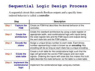
EE 3563 Sequential Logic Design Principles. A sequential logic circuit is one whose outputs depend not only on the current inputs, but also on the past sequence of inputs, possibly arbitrarily far back in time The book gives the example of changing channels on a TV

E N D
EE 3563 Sequential Logic Design Principles • A sequential logic circuit is one whose outputs depend not only on the current inputs, but also on the past sequence of inputs, possibly arbitrarily far back in time • The book gives the example of changing channels on a TV • A TV with a remote – the old manual dial doesn’t count • A computer would be a more complex example • Can not describe the behavior of a sequential circuit with a simple truth table – output as a function of input • Must know the “state” of the circuit • Collection of state variables whose values at any one time contain all the information necessary to determine the future behavior • In the TV example, the current channel must be known in order to increment/decrement the channel EE 3563 Digital Systems Design
EE 3563 Sequential Logic Design Principles • A state variable describes the value of a particular element of a sequential circuit • In the TV example, a state variable would be needed to store the current channel • Could be stored internally any number of ways • 3-digit BCD • Binary number • In digital circuits a state variable has two values • The total number of possible states is 2n where n is the number of binary state variables • You can see that this number can grow large very quickly, but it is finite • Sequential circuits often called finite-state machines • Often, it is impractical to test every possible state transitioning to every other possible state • Say a 3-digit BCD is used for the TV, that’s 12 bits or 4096 states • Would not test every channel change combination EE 3563 Digital Systems Design
EE 3563 Sequential Logic Design Principles • State changed occur when the internal clock transitions • The clock is active high when the state change occurs on the rising edge or at a high value • The clock is active low when the state change occurs on the falling edge or when the clock is low • More on rising/falling edges later • Some circuits are designed so some elements are triggered by an active high clock while other elements are triggered by an active low • The clock period (T) is the time between successive changes • The clock frequency is the inverse of the period (f = 1/T) • Frequency of 44.1 KHz has a period of 22.58 μs EE 3563 Digital Systems Design
EE 3563 Sequential Logic Design Principles • The first edge in a clock pulse is called the clock tick • State changes occur in lock-step with the clock • Some circuits, called asynchronous circuits, do not completely change state on the tick of the clock, but rather various elements “signal” other elements when they are ready • How do you suppose the TV example implements a clock? EE 3563 Digital Systems Design
EE 3563 Sequential Logic Design Principles • The first edge in a clock pulse is called the clock tick • State changes occur in lock-step with the clock • Some circuits, called asynchronous circuits, do not completely change state on the tick of the clock, but rather various elements “signal” other elements when they are ready • How do you suppose the TV example implements a clock? • It doesn’t! Not all sequential circuits require a clock! • The duty cycle is the percentage of time a clock signal is asserted • Does NOT have to be symmetrical EE 3563 Digital Systems Design
EE 3563 Sequential Logic Design Principles • Clock Signal EE 3563 Digital Systems Design
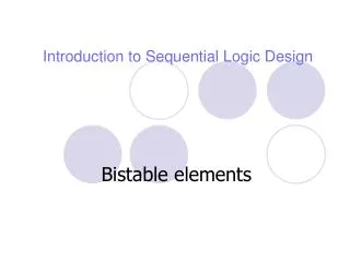
EE 3563 Sequential Logic Design Principles • Bistable elements have two stable states • The simplest bistable circuit element is shown below • Upon power up, what will be the outputs? EE 3563 Digital Systems Design
EE 3563 Sequential Logic Design Principles • Bistable elements have two stable states • The simplest bistable circuit element is shown below • Upon power up, what will be the outputs? • It is analogous to flipping a coin, which could have 1 of 3 possible outcomes, not all equally likely • Heads, Tails, on its side EE 3563 Digital Systems Design
EE 3563 Sequential Logic Design Principles • Graph shows behavior of the inverters • Two stable states, one metastable state • In the metastable state, a little noise or power spike could cause the outputs to transition to one of the stable states • Just like a little vibration could cause the coin that landed on its side to fall over EE 3563 Digital Systems Design
EE 3563 Sequential Logic Design Principles • Another metastable example • All sequential circuits are susceptible to metastable behavior • This situation manifests itself in situations when the triggering actions for latches and flip flops are marginal • For example, if the clock speed is too high for a particular circuit EE 3563 Digital Systems Design
EE3563 Latches and Flip-Flops • Latches and flip-flops are the basic building blocks of most sequential circuits • Flip-flops use a clocking signal to change state • Latches change output at any time , independent of a clocking signal • This is the distinction made by the text • Some texts have been known to use the terms incorrectly, calling a flip-flop a latch • The distinction is important for correct operation of some sequential circuits EE 3563 Digital Systems Design
EE3563 Latches and Flip-Flops • S-R (Set-Reset) Latch implemented with NOR gates • S sets Q to one, R resets (clears) Q to zero • Function Table describes the behavior • Doesn’t tell the whole story • Metastable behavior not indicated • Use the functional behavior timing diagram • Note: QN is not always the complement of Q EE 3563 Digital Systems Design
EE3563 Latches and Flip-Flops • Functional behavior of an S-R latch • Note the (undesirable) metastable behavior • May enter that state if S and R are negated simultaneously • Since nothing is perfectly “simultaneous” the designers often specify how “close” is considered simultaneous • Usually specified as within 20 ns, but may be different for faster/slower circuits EE 3563 Digital Systems Design
EE3563 Latches and Flip-Flops • The S’-R’ Latch – called the S-bar R-bar latch • I don’t have an “overline” in MS Word • Similar to S-R latch, except it has active low sets/resets • May be built from NAND gates • Remembers its state when both inputs are one • When both inputs go to zero, outputs both go to one EE 3563 Digital Systems Design
EE3563 Latches and Flip-Flops • The S-R Latch with enable • When the enable input “C” is asserted, behaves just like an S-R latch • When C is deasserted, it remembers its current values • May become metastable if both inputs are one and C goes to zero (deasserted) EE 3563 Digital Systems Design
EE3563 Latches and Flip-Flops • The D (data) latch allows the storage of data • Avoids the metastable problem better than the S-R latch • It is essentially an S-R latch with enable and the S input tied to an inverter feeding the R input • The “C” enable input may also be a clock input • When enabled, the latch is transparent EE 3563 Digital Systems Design
EE3563 Latches and Flip-Flops • The D latch does not eliminate the metastability problem • Four delay parameters are shown • tpLH(CQ) – time propagation from L to H of Q due to input C • When C is transitioning to zero, the data must be stable for tsetup and thold to avoid metastability problems EE 3563 Digital Systems Design
EE3563 Latches and Flip-Flops • Once you use the enable input with a clocking signal, you are working with a flip-flop instead of a latch • We can construct a positive-edge-triggered D flip-flop with a pair of D latches as shown below • It will only change output on the rising edge of the clock • If the input changes while the clock is high, the output will not change triangle indicates edge-triggered behavior EE 3563 Digital Systems Design
EE3563 Latches and Flip-Flops • The edge-triggered D flip-flop also has a setup and hold time • If the setup/hold time is not met, the edge-triggered FF will usually become stable (though in an unpredictable state) • It can go metastable or oscillate • Can also have a negative edge-triggered FF • Some D flip-flops have separate set/reset inputs to force the output to a particular state EE 3563 Digital Systems Design
EE3563 Latches and Flip-Flops • Negative edge-triggered D-FF EE 3563 Digital Systems Design
EE3563 Latches and Flip-Flops • Edge-triggered D-FF with Preset and Clear EE 3563 Digital Systems Design
EE3563 Latches and Flip-Flops • Edge triggered D-FF with enable • This can be used to hold a value despite the clock signal EE 3563 Digital Systems Design
EE3563 Latches and Flip-Flops • A scan flip-flop is used for testing • Use an alternate source of data during testing • When in testing mode, a pattern can be scanned into all the flip-flops • After loading the test pattern, the flip-flops are put into normal mode and clocked as usual • Two extra inputs are used • Test enable which is simply a pin used to choose between the normal input and the test input • Test input – the alternate D input • All the different flip-flops could be designed with a scan capability EE 3563 Digital Systems Design
EE3563 Latches and Flip-Flops • Scan flip-flops EE 3563 Digital Systems Design
EE3563 Latches and Flip-Flops • Master/Slave S-R Flip-Flops • Used when we want an S-R FF to change only in synchronization with a clock • Can use S-R latches in place of D latches of the negative edge-triggered flip-flop • Resulting device is not edge triggered because the output depends on the value during the entire time the clock is high • A short pulse can set or reset the master latch • The final output depends upon whether the master latch was set/reset while the clock was high • Changes output to final latched value – value at falling edge of clock • Called a pulse-triggered flip-flop EE 3563 Digital Systems Design
EE3563 Latches and Flip-Flops • Master/Slave S-R pulse triggered flip-flop • Metastable behavior occurs if pulsed when both S-R are high postponed output indicator Master Slave S-R Flip-Flop S-R Flip-Flop EE 3563 Digital Systems Design
EE3563 Latches and Flip-Flops • Master/Slave J-K Flip-Flop • Solves the problem of when both S and R are asserted simultaneously • J & K inputs are analogous to S-R inputs • However, asserting J asserts the master’s S input only as long as the QN output is one (Q is zero) • Asserting K asserts the master’s R input only if Q is one • If both are asserted at the same time, the flip-flop goes to the opposite of its current state • problem: it is possible for the output to change to a one even though K and not J is asserted at the end of the triggering pulse • Called 1’s catching • Also may have a 0’s catching • J-K inputs MUST be held valid during entire period clock is 1 EE 3563 Digital Systems Design
EE3563 Latches and Flip-Flops • Master/Slave J-K flip-flop EE 3563 Digital Systems Design
EE3563 Latches and Flip-Flops • Edge-triggered J-K flip-flop • Solves the 1’s catching and 0’s catching problem (as well as the simultaneous input change problem) • Inputs sampled at the rising edge • Have obsoleted the pulse-triggered types • 74x109 is a positive edge-triggered J-K’ flip-flop • K is active low EE 3563 Digital Systems Design
EE3563 Latches and Flip-Flops • A T (toggle) flip-flop changes state upon every tick of the clock • May be pos/neg edge-triggered and have an enable • Can be used as a frequency divider • Use one T-FF to divide by two, cascade them for larger divisions EE 3563 Digital Systems Design