Download
1 / 25
250 likes | 260 Views
This document provides an overview of the appliedVHDL system design, including the context diagram, functional partition, and system elements. It also includes a glossary of relevant terms. Use the provided links to navigate the design hierarchy and perform exercises.

E N D
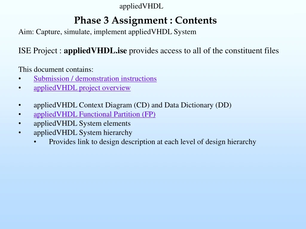
Phase 3 Assignment : Contents • Aim: Capture, simulate, implement appliedVHDL System • ISE Project : appliedVHDL.ise provides access to all of the constituent files • This document contains: • Submission / demonstration instructions • appliedVHDL project overview • appliedVHDL Context Diagram (CD) and Data Dictionary (DD) • appliedVHDL Functional Partition (FP) • appliedVHDL System elements • appliedVHDL System hierarchy • Provides link to design description at each level of design hierarchy
Context Diagram SRAM Spec DFD0.0 ramBFM appliedVHDL Data Dictionary: same signals as for appliedVHDLV1 top level, with the addition of SRAM signals (refer to the SRAM specification document)
System Elements appliedVHDL Functional Partition (FP) Project Element Activity (ref glossary)IOCSRBlk contains IOCtrlr: Serial (UART) interface and I/O controller C, FSM, S, I Parses host GUI commands and dataCSRBlk: Control and status register block Completed (phase 2)memCtrlr: SRAM datapath select and SRAM controller FSM C, FSM, S, BFMdatCtrlr: Datapath (8-bit UART 32-bit SRAM C, S, Idata bundle and vice–versa) dspBlk: Image pixel subtractor (delta-frame generation) C, FSM, S appliedVHDL (top level): Complete appliedVHDL system C, S, INUIGProject: contains IOCSRBlk, datCtrlr, DSPBlkUART Xilinx UART component ProvideddisplayCtrlr: Multiplexed 7-segment display and LED controller Completed (phase 1) Glossary : FSM : Finite State Machine C : VHDL CaptureS : Simulation I : ImplementationBFM: VHDL Bus Functional Model
System Hierarchy Use the active links to browse the design hierarchy and documentation Perform exercises P3.* in sequence, reviewing the associated design documentationISE Project : appliedVHDLV1.ise (provides access to all of constituent files) L15 P3.9 CD, FP, DD, DFD0.0, PD0.0, DD0.0 P3.9 NUIGPackage details P1 P3.7 P3.8 DFD2.0 DFD1.0, DD1.0 DFD3.0 P3.2 P3.5 P3.4(B) P3.6 DFD1.2 DFD1.3 DFD1.4 DFD1.1, DD1.1, PD1.1 DFD1.1.1 P3.3(B) P2.1 P3.3(A) P3.4(A) DFD1.3.1 DFD1.1.2 1.3.2 P3.3(C) ramBFM
Data Flow Diagram (appliedVHDL DFD 0.0) DFD 1.0 SRAM Spec ramBFM DFD 2.0 DFD 3.0
DFD 0.0 appliedVHDL Process Description • Handshakes with host via UART byte interface • Decodes UART control/data byte sequence and selects • Accesses R/W 8 byte-wide CSRs (Control and Status Registers) • Performs SRAM • write access : • Bundles data from UART into 32-bit longword • Performs single longword (32-bit) SRAM write • read access : • Single longword (32 bit) SRAM read • Unbundles SRAM 32-bit longword into four separate bytes and transfers to UART • Performs DSP task (delta frame generation using pixel-by-pixel subtraction) placing result in SRAM for subsequent reading by host via UART byte interface (process 2.0). • displayCtrlrl (process 3.0) displays various signals on 7-segment displays and LEDS to aid hardware debug.
DFD 0.0 Incremental Data Dictionary • rxDat(7:0) : byte-wide data generated by UART from serial byte received from host. rxDat is validated by assertion (h) of rxDatValid • rxDatValid :assertion (h) validates rxDat(7:0). Signal remains asserted until assertion of rxDatAck • rxDatAck : assertion by FPGA acknowledges receipt of a valid rxDat byte. Signal asserts for one clock period only • txDat(7:0) : byte-wide data generated by FPGA and transferred to UART for serialisation and transfer to host PC. txDat is validated by assertion (h) of txDatValid • txDatValid : assertion (h) validates txDat(7:0) • rTxDat: registered txDat(7:0) (on assertion of txDatValid) to enable stable display of txDat on h/w dvp system 7-seg display for aiding debug
DFD 1.3 SRAM SpecramBFM DFD 1.4 DFD 1.2 DFD 2.0 DFD 1.1 DFD 3.0
NUIGProject DFD 1.0 Incremental Data Dictionary • dPathDone: decode of count=0. Assertion indicates that either : 4 bytes are available to write as 32-bit RAM data or 4 bytes have been transferred to UART from 32-bit RAM data • ldIODat2RamReg : assertion synchronously loads 32-bit RAM data register for RAM write • datFromRam(31:0) 32 bit data read from RAM • IORamWr : IO subsystem RAM write access control signal • IORamRd : IO subsystem RAM read access control signal • IODat2Ram(31:0) : 32 bit IO subsystem data to be written to RAM • IORamAdd(17:0) : 18 bit RAM address (from IO subsystem). Max RAM address is 256k • ramDone : ram r/w access completion flag • dspRamWr : dspBlk subsystem RAM write access control signal • dspRamRd : dspBlk subsystem RAM read access control signal • dspDat2Ram(31:0) : 32 bit data dspBlk subsys data to be written to RAM • dspRamAdd(17:0) : 18 bit RAM address (from dspBlk subsystem). Max RAM address is 256k • dspActive : dspBlk active flag • dspDone : dspBlk task completed flag • dspAddRange(15:0) : no. of RAM locations to be accessed by dspBlk task
NUIGProject DFD 1.0 Incremental Data Dictionary • csrTask : flag indicating that CSR read or write access is in progress • CSR: array of CSR bytes (used to control elements of system. The CSR block does not currently perfoms any subsystem status function, though could be developed to do so. Array type is defined as follows: type byteArray is array (7 downto 0) of std_logic_vector(7 downto 0); • csrOut : selected CSR byte for read or write • ldByteCnt : assertion synchronously loads 3 into 4 state down counter used to determine (when count is 0) when - 4 bytes are available to write as 32-bit RAM data or - 4 bytes have been transferred to UART from 32-bit RAM data The following signals are used internally but equivalent to output signals, since cannot use a signal ofmode OUT on right hand side of assignment, equivalence check or inside the VHDL port map : • intTxDatValid : assertion validates txDat byte (to UART) • intRxDatAck : assertion acknowledges receipt of byte data (rxDat) from UART
DFD 1.1 IOCSRBlk CSRBlk (DFD 1.1.2) completed during Phase 2 symbol DFD 1.1.1 DFD 1.1.2
DFD 1.1 (IOCSRBlk) Incremental Data Dictionary • regCSRInfo : assertion (on detection of valid control byte) registers rxDat(6:4) as csrAdd(2:0) register registers csrAdd(1) as csrTask • clrCSRInfo : assertion clears csrTask flag
DFD 1.1 (IOCSRBlk) Process Description • IOCtrlr Finite State Machine, command register and CSRBlk elements • Decodes UART control/data byte sequence • Handshakes with host via UART byte interface • CSR access : provides Control and Status Register (CSR) read/write access (8 byte-wide CSRs) • SRAM Access : activates datCtrlr module. Provides clear and increment signals to datCtrlr 4-state counter for byte-to-32-bit bundling and vice versa. • Activates DSP task and waits for acknowledgement of task completion
DFD 1.1.1 IOCtrlr & cmdReg Process Description, Functional Partition and FSM IOCtrlr FSM manages the appliedVHDL system behaviour processes cmd bytes received on serial port from host GUI (master)
IOCtrlr FSM description Refer to FSM flowchart (next slide) • Finite State Machine (FSM) detects and processes control or data byte (rxDat) from UART (on assertion of rxDatValid signal). • Decodes : • CSR access : • Registers csrAdd(2:0) and csrTask flag • write : requires a further data byte (on rxDat) from UART • read : provides CSR data byte (csrOut) to UART on txDat • RAM access : • Requires RAM address to be written to CSR(2:0) bytes • CSR(2) = XXXXXX ramAdd(17:16) (X : unused CSR bit) • CSR(1) = ramAdd(15:8) • CSR(0) = ramAdd(7:0) • write : requires four further data byte (on rxDat) from UART to produce a 32-bit longword for RAM write • read : provide four unbundled data byte (extracted from 32-bit RAM longword) to UART (on txDat) • Activates dspBlock (dspActive) and waits for dspDone assertion indicate completion. • Validates byte data transmission to UART (txDatValid assertion) • Acknowledges receipt of byte data (rxDat) from UART (rxDatAck assertion)
DFD 1.3 SRAM SpecramBFM DFD 1.4 DFD 1.2 DFD 2.0 DFD 1.1 DFD 3.0
DFD 1.2 (datCtrlr) : assignment instructions datCtrlr level • Capture the datCtrlr.vhd VHDL model. The lab file contains commented VHDL template files • Check VHDL code syntax, synthesise and view RTL schematic. Confirm correctness. • Simulation is not required. datCtrlr will be simulated after integration at appliedVHDL level. • Implementation on FPGA is not required
DFD 1.2 (datCtrlr) Process Description • During an SRAM write : • bundles 4 data bytes from UART as 32-bit SRAM longword • Selects CSR byte data to output to UART • During an SRAM read : • unbundles 32-bit SRAM data into 4 data bytes for sending to UART • Selects unbundled RAM byte data to output to UART • Use 4 level counter to maintain control of bundle/unbundle sequence • Counter loaded and incremented by IOCtrlr state machine • rTxDat : registered version of valid txDat(7:0) value (on assertion of txDatValid). rTxDat value can be displayed on the 7-segment display to aid hardware debug
DFD 1.4 (datCtrlr) Data Dictionary • byteCnt : • Counter value, loaded with 3, integer (0 to 3) • Counts downwards to 0, decrementing on the following conditions : • assertion of rxDatAck, i.e, new byte received from UART for bundling for RAM write • assertion of txDatValid, i.e, new byte unbundled and transmitted to UART after RAM read. • Count value 0 indicates completion of bundle or unbundle task. • unbundledRamDat : Unbundled byte from RAM data, available for sending to UART • rTxDat : registered version of valid txDat(7:0) value (on assertion of txDatValid).
appliedVHDL : assignment instructions • appliedVHDL level • Review the appliedVHDL.vhd VHDL model. • Simulate appliedVHDL_TB.vhd fully, review the timing waveform and verify correct VHDL model operation. • Implementation on FPGA is not required • Implement on FPGA • Review appliedVHDL.ucf (provided) for pinout • Implement appliedVHDL on the Spartan 3 development system and test
Write 0 to CSR(0->2),write C3C2C1C0 longword to SRAM (loc 0)rd longword from SRAM
rd longword from SRAM C3C2C1C0