Download
1 / 3
40 likes | 135 Views
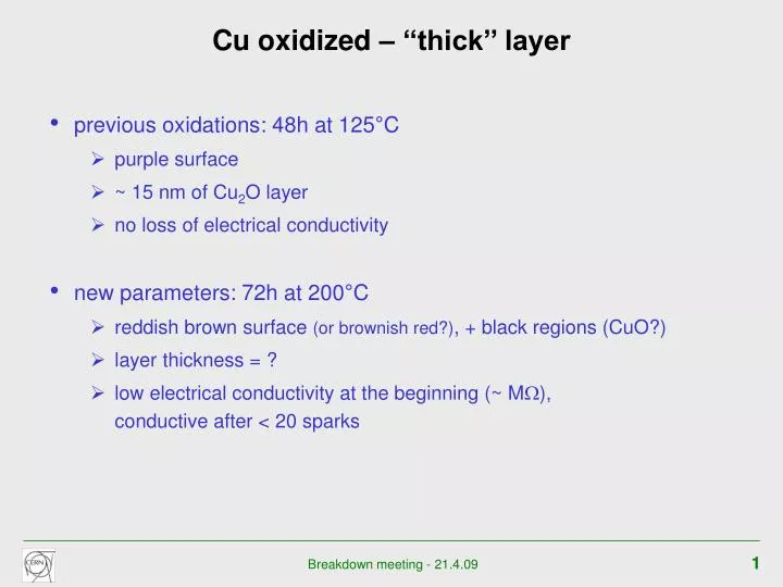
Cu oxidized – ‘‘thick’’ layer. previous oxidations: 48h at 125°C purple surface ~ 15 nm of Cu 2 O layer no loss of electrical conductivity new parameters: 72h at 200°C reddish brown surface (or brownish red?) , + black regions (CuO?) layer thickness = ?

E N D
Cu oxidized – ‘‘thick’’ layer • previous oxidations: 48h at 125°C • purple surface • ~ 15 nm of Cu2O layer • no loss of electrical conductivity • new parameters: 72h at 200°C • reddish brown surface (or brownish red?), + black regions (CuO?) • layer thickness = ? • low electrical conductivity at the beginning (~ MW), conductive after < 20 sparks
Cu oxidized – ‘‘thick’’ layer • similar results until now (tests are still running) possible slight gain with increased thickness
… the first spot was really bad at the beginning (with a completely oxidized anode) Cu oxidized – ‘‘thick’’ layer • BUT...