Download
1 / 37
440 likes | 783 Views
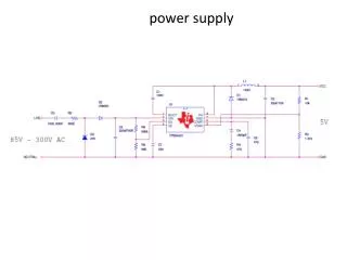
Switching Power Supply. Team 22 Tony Lin Hsin-Cheng Yao TA: Chad Carlson ECE 445 Fall 2004 12/01/2004. Switching Power Supply. Conversion from AC voltage to DC voltage A smart regulator Crucial component in many electronic devices such as computer and its peripherals . Benefits of SPS.

E N D
Switching Power Supply Team 22 Tony Lin Hsin-Cheng Yao TA: Chad Carlson ECE 445 Fall 2004 12/01/2004
Switching Power Supply • Conversion from AC voltage to DC voltage • A smart regulator • Crucial component in many electronic devices such as computer and its peripherals
Benefits of SPS • High efficiency and less heat generation • Tighter regulation • Smaller size and weight
AC Input • The AC input is simply the commercial AC power supply, a plug is connected to our device input for users to simply connect our product to outlets on the wall.
Flyback Converter Vout/Vin = (N2/N1) * D/(1-D)
Transformer • Core Geometry: E-E • Core Model: EE 25/18 • N1:N2:N3 = 108:12:18
Duty Ratio Control • Duty ratio represents the on-time of the nMOS switch
Two Cases that Cause the Duty to Change • When input voltage changes • When load changes
Case 1: When input voltage changes with constant load at 10 ohms
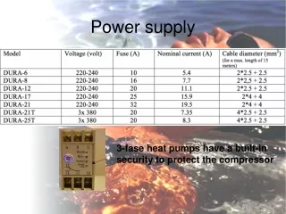
The Load Electronic Load
PWM Control of the nMOS Switch • PWM regulates the on or conduction time of the switching transistor. • As the width of the pulse is increased, the switching transistor stays on longer, and more energy is applied to the switching transformer. This produces an increase in the DC output current.
Power Loss • The three parts of the circuits that contribute to the most power dissipation
Bridge Rectifier • The reverse diodes in the bridge rectifier consumes power • A power dissipation of 4.7W at maximum current from the spec sheet • Prectifier ~ 1.5W for our circuit
Transformer • The Core Loss in Transformer • Hysteresis Loss and Eddy Current Loss • Ptransformer = P0 fa Bb
nMOS Switch • Conduction Loss • Switching Loss • Pswitching loss = f Voff Ion (ton + toff) / 6 • Pswitching loss ~ 2W for our circuit
Challenges and Success • Grounding Problem • Regulated Output and Close-to-Proposed Efficiency
Recommendations • Find another nMOS switch with a lower power dissipation • Use of “pot-cores” for transformer • Double fuses on the input end to better protect the circuits
References • Elements of Power Electronics, Krein • Phillips UC3842 Datasheet • Understanding Switch Mode Power Supplies, Sencore Tech Tips • Switching Regulators, WebEE.com
Acknowledgements • Special thanks to Chad throughout the whole project and showing the “damages” done on our diodes under microscope • Professor Swenson • Professor Chapman for advices • Brett and Zach, the Power TAs
Q & A Thank You!