Download
1 / 27
270 likes | 738 Views
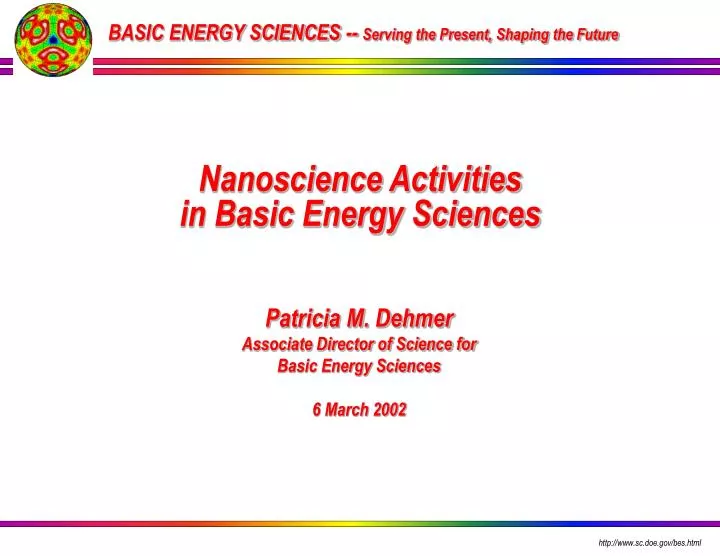
BASIC ENERGY SCIENCES -- Serving the Present, Shaping the Future Nanoscience Activities in Basic Energy Sciences Patricia M. Dehmer Associate Director of Science for Basic Energy Sciences 6 March 2002 http://www.sc.doe.gov/bes.html The Scale of Things -- Nanometers and More 1 cm 10 mm

E N D
BASIC ENERGY SCIENCES -- Serving the Present, Shaping the Future Nanoscience Activities in Basic Energy Sciences • Patricia M. Dehmer • Associate Director of Science for • Basic Energy Sciences6 March 2002 http://www.sc.doe.gov/bes.html
The Scale of Things -- Nanometers and More 1 cm 10 mm 10-2 m Head of a pin 1-2 mm 21st Century Challenge 1,000,000 nanometers = 10-3 m Ant ~ 5 mm 1 millimeter (mm) Microwave Dust mite 200 mm 0.1 mm 100 mm 10-4 m Fly ash ~ 10-20 mm Human hair ~ 10-50 mm wide 0.01 mm 10 mm The Microworld 10-5 m Infrared Red blood cells with white cell ~ 2-5 mm 1,000 nanometers = 10-6 m 1 micrometer (mm) Visible 0.1 mm 100 nm 10-7 m Combine nanoscale building blocks to make novel functional devices, e.g., a photosynthetic reaction center with integral semiconductor storage Ultraviolet 0.01 mm 10 nm The Nanoworld 10-8 m Nanotube transistor Nanotube electrode ~10 nm diameter ATP synthase 10-9 m 1 nanometer (nm) Soft x-ray DNA ~2-1/2 nm diameter 10-10 m 0.1 nm Carbon nanotube ~2 nm diameter Quantum corral of 48 iron atoms on copper surface positioned one at a time with an STM tip Corral diameter 14 nm Things Natural Things Manmade MicroElectroMechanical devices 10 -100 mm wide Red blood cells Pollen grain Zone plate x-ray “lens”Outermost ring spacing ~35 nm Atoms of silicon spacing ~tenths of nm Office of Basic Energy Sciences Office of Science, U.S. DOE Version 03-05-02
Nanoscience and Nanotechnology • The nanoscale is not just another step towards miniaturization. It is a qualitatively new scale where materials properties, such as melting point or electrical conductivity, differ significantly from the same properties in the bulk. • “Nanoscience” seeks to understand these new properties. • “Nanotechnology” seeks to develop materials and structures that exhibit novel and significantly improved physical, chemical, and tribiological properties and functions due to their nanoscale size. • The goals of nanoscience and nanotechnology are: • to understand and predict the properties of materials at the nanoscale • to “manufacture” nanoscale components from the bottom up • to integrate nanoscale components into macroscopic scale objects and devices for real-world uses
The National Nanotechnology InitiativeAddressing both scientific frontiers and national needs Sep 1998 The Interagency Working Group on Nanoscience, Engineering, and Technology (IWGNSET) formed by the NSTC. The IWG meets monthly.Participating agencies: NSF, DOE, DOD, NIH, NASA, DOC/NIST and later alsoCIA, DOJ, DOS, DOT, DOTreas, EPA, NRC, USDA Aug 1999 The IWG releases National Nanotechnology Initiative (NNI) report after extensive input from the scientific communityAug-Nov 1999 BES reportsComplex Systems: Science for the 21st Centuryhttp://www.sc.doe.gov/production/bes/complexsystems.htmNanoscale Science, Engineering and Technology Research Directionshttp://www.sc.doe.gov/production/bes/nanoscale.htmlSep-Oct 1999 The six principal agencies brief OMB and a PCAST panel charged to the review the proposed NNIFeb 2000 The NNI is initiated as part of the FY 2001 budget requestFall 2001- National Academy of Sciences reviews the NNI activitiesSpring 2002
NNI FY 2003 Funding RequestsDOE is one of the three lead agencies National Nanotechnology Initiative (NNI Coordination Office compilation, as of 1/18/02) FY 2003 (Dollars in millions) 221.0 NSF 201.0 DOD 139.3 DOE All other agencies 117.4 TOTAL NNI 678.7 *Excludes funding for synchrotron light source and neutron scattering facility operations and beamlines. * + up to $15M in FY 02
National Nanotechnology Initiative Focus Areas (BES activities shown in bullets) • Long-term, fundamental nanoscience and engineering research • FY 2001: BES awarded $26.5M in new NNI funds based on peer review -- 76 university grants ($16.1M) and 12 laboratory awards ($10.4M) • FY 2002: BES may award up to $15M based on peer review • Centers and networks of excellence • BES Nanoscale Science Research Centers – the DOE “flagship” NNI activity • Research infrastructure • BES supports the synchrotron light sources, neutron scattering facilities, and other specialized facilities in support of nanoscale science • Grand challenge areas • Nanostructured materials “by design” – stronger, lighter, tougher, harder, self-repairing, and safer • Efficient energy conversion and storage • Nanoelectronics, optoelectronics, and magnetics • National security • Chemical/biological/radiological/explosive (CBRE)detection/protection • Nanoscale processes for environmental improvement • Economical and safe transportation • Advanced healthcare, therapeutics, and diagnostics • Microcraft space exploration and industrialization • Ethical, legal, societal implications and workforce education and training • Graduate and postdoc training supported via university grants and lab awards
Nanoscale Science and Technology …… in the Bush Administration Science Based Science Policy Meeting of the American Association for the Advancement of ScienceJohn MarburgerFebruary 15, 2002 (Excerpts) The quantum technologies of the chemistry and physics of atoms, molecules, and materials developed rapidly through several generations during the Cold War. By 1991, when the Soviet Union finally dissolved, scientists were beginning to wield instruments that permitted the visualization of relatively large-scale functional structures in terms of their constituent atoms. The importance of this development cannot be over-stated. … The result is an unprecedented ability to design and construct new materials with properties that are not found in nature. The revolution I am describing is one in which the notion that everything is made of atoms finally becomes operational.
The picture of science I have portrayed -- and I am aware that it is only part of science, but an important part -- has immediate implications and challenges for science policy. First, there is the need to fund the enabling machinery for exploring the frontier of complexity. Some of this machinery is expensive, such as the great x-ray sources operated by the Department of Energy, or the Spallation Neutron Source. Even the computing power required at the frontier is expensive and not yet widely available to investigators. Second is the desirability of funding research in the fields that benefit from the atomic level visualization and control of functional matter. They fall into the two categories of organic and inorganic. We call them biotechnology and nanotechnology. I like to think of biotechnology as organic nanotechnology. Third, there is the very serious problem of the inadequacy of resources to exploit all the new opportunities that now lie before us along the vast frontier of complexity. The need for choice, and for wise allocation of resources to seize the most advantage for society from our leadership in these fields, is a strong motivation for better planning and management of the nation’s science enterprise.
Nanoscale Science Research Centers (NSRCs) • NSRCs: • Research facilities for synthesis, processing, and fabrication of nanoscale materials • Co-located with existing user facilities (synchrotron radiation light sources, neutron scattering facilities, other specialized facilities) to provide characterization and analysis capabilities • Operated as user facilities; available to all researchers; access determined by peer review of proposals • Provide specialized equipment and support staff not readily available to the research community • Conceived with broad input from university and industry user communities to define equipment scope • NSRCs have been extensively reviewed by external peers and by the Basic Energy Sciences Advisory Committee
Date Activity FY 2000 FY 2001 FY 2002 1999-present BESAC reviews NSRC concept and develops philosophy for their establishment December 2000 Proposals for NSRCs received ANL, BNL, LBNL ORNL, SNL/LANL write and submit proposals April 2001 Mail peer review and panel review of proposals from ANL, BNL, LBNL, ORNL, and SNL/LANL to establish CD0 (Justification of Mission Need) LBNL, ORNL, SNL/LANL receive CD0 approval (6/13/01) December 2001 Lehman review of Conceptual Design Reports (CDR) for LBNL, ORNL, and SNL/LANL using both a cost, schedule, scope, & construction management review team and a scientific review team. Scientific review team considers comments from the April 2001 review and from BESAC. ORNL CDR approved. PED and construction funding requested for FY 03. CD1 signed (2/22/02), allowing use of PED funds. LBNL and SNL/LANL requested to do additional work before CDR is approved. Based on review, CD1 expected in May 2002, allowing use of PED funds during last quarter of FY 02. PED funding, but no construction funding, requested for FY 03. February 2002 Mail peer review of resubmitted proposals from ANL and BNL to establish CD0 April 2002 Lehman re-review of CDRs for LBNL and SNL/LANL using cost, schedule, scope, & construction management review team only NSRC Timeline
Electron Microscopy Center for Materials Research Advanced Photon Source Materials Preparation Center Center for Microanalysis of Materials Advanced Light Source Intense Pulsed Neutron Source National Center for Electron Microscopy National Synchrotron Light Source Molecular Foundry Spallation Neutron Source Stanford Synchrotron Radiation Lab Center for Nanophase Materials Sciences Linac Coherent Light Source Surface Modification & Characterization Center Combustion Research Facility Los Alamos Neutron Science Center Shared Research Equipment Program High-Flux Isotope Reactor Center for Integrated Nanotechnologies James R. MacDonald Lab Pulse Radiolysis Facility NSRCs ( ) and the BES User Facilities • 4 Synchrotron Radiation Light Sources • Linac Coherent Light Source (CD0 approved) • 4 High-Flux Neutron Sources (SNS under construction) • 4 Electron Beam Microcharacterization Centers • 5 Special Purpose Centers • 3 Nanoscale Science Research Centers (CD0s approved) Under construction In design/engineering In design/engineering
Stanford Synchrotron Radiation Laboratory BES X-ray and Neutron Scattering Facilities Advanced Photon Source Intense Pulsed Neutron Source Advanced Light Source National Synchrotron Light Source Spallation Neutron Source Manuel Lujan Jr. Neutron Scattering Center High-Flux Isotope Reactor
Multistory Lab/Office Building Nanofabrication Research Lab The Center for Nanophase Materials SciencesOak Ridge National Laboratory Unique tools and capabilities: • World’s absolute best neutron scattering capabilities are provided by the Spallation Neutron Source and the newly upgraded High-Flux Isotope Reactor Scientific focus areas: • Nanoscale materials related to polymers, macromolecular systems, exotic crystals, complex oxides, and other nanostructured materials • Scientific theory/modeling/simulation, building on the outstanding ORNL materials sciences program SNS HFIR Center for Nanophase Materials Sciences
21st Century Challenge Combine nanoscale building blocks to make functional devices, e.g., a photosynthetic reaction center with integral semiconductor storage The Molecular FoundryLawrence Berkeley National Laboratory Unique tools and capabilities: • Advanced Light Source • National Center for Electron Microscopy • National Energy Research Scientific Computing Center • Nationally unique facilities, such as thee-beam nanowriter – nanofabrication facility • Outstanding faculty and students in multidisciplinary research, including materials science • physics • chemistry • biochemistry • biomolecular materials • engineering Scientific focus areas: • Combination of “soft” and “hard” materials/building units • Multicomponent functional assemblies
Nano-Electronics, and Photonics 2-D GaAs/AlGaAs 3-D 180nm Silicon Photonic Lattices Nano-Mechanics Nano/Bio/ Micro Deformations are quantized by dislocation interactions Bio-Tailored Surfaces The Center for Integrated NanotechnologiesSandia National Laboratories (Albuquerque) and Los Alamos National Laboratory Unique tools and capabilities: • Compound Semiconductor Laboratory (SNL) • Microelectronics Development Laboratory (SNL) • Nano lithography, imaging, and characterization; MEMS (SNL) • Los Alamos Neutron Science Center (LANL) • National High Magnetic Field Lab (LANL) • Computing/theory (LANL) Scientific focus areas: • Nanophotonics and nanoelectronics • Electronic, magnetic, and optical phenomena at nanoscale • Nanomechanics • Mechanisms and limits of mechanical deformation • Unique mechanical properties occurring at the nanoscale • Nano-micro interfaces • Bridging functional nanoassemblies to micro (and larger) world
Molecular Perfection: The Fullerene Nanotube • The strongest fiber that will ever be made • Electrical conductivity of copper or silicon • Thermal conductivity of diamond • The chemistry of carbon • The size and perfection of DNA • Can we harness this material?
Materials with Enhanced Functionality via Nanostructuring Layered-Structures Nanocrystals Nanocomposites • Electronics/photonics • Novel Magnets • Tailored hardness • Catalysts • Tailorable light emission • Supercapacitors • Separation membranes • Adaptive/responsive behavior • Pollutant/impurity gettering Nanoscience enables scientifically tailored materials
Vertical Cavity Surface Emitting Lasers (VCSELs) Photonic Lattices poly-Si Si substrate Materials with New Optical Properties via Nanostructuring A 2-D B • The VCSEL is to photonics what the transistor was to electronics. A key 21st century technology • Most efficient, low-power light source (57% in ‘97) • Applications in stockpile stewardship, optical communications, scanners, laser printing, computing... 3-D • Optical signals guided through narrow channels and around sharp corners • Near 100% transmission • Key technology for telecommunications and optical computing
The Promise of Addressing Old Problems in New Ways Semiconductor nanocrystals linked to bio-molecules light-up a cell’s actin filaments (red) and nucleus (green) • Nanocrystals of CdSe fluoresce with different colors depending only on their size • Different sized crystals can be selectively bound to different parts of a cell or to any desired structure to “light up” the parts • Biological labeling • Molecular processes in cells
Materials for Improved Energy Efficiency and Performance Exchange-Spring MagnetsSmCo/Fe Ion-Implantation MetallurgyAl+O Implanted Ni 2-nm Al2O3 particles • Tailorable magnetic properties • Lighter, stronger magnets • More efficient motors • Superior strength • Hard thin layers • Greatly reduced friction & wear
3-D Self-Assembled Materials via Nanostructuring Self-Assembled Monolayers on Mesoporous Supports • Chemically selective surfactant molecules self-assemble within the interstices of a mesoporous silica matrix derived through solution processing routes. • Resulting material shows high adsorption capacity for mercury and other heavy metals. • Numerous environmental and commercial applications. 55 nm pore diameter, 900 m2/gm surface area
Ultimate “Lab on a Chip” Nanophotonics/Nanoelectronics Complex Functional Materials Electronics MOS IC Fluidic Bio-Pump New properties New functions New Science LED display LED display Mechanically positioned mirrors Laser Emitter Arrays Micro - fluidic channels Microfluidic channels Nano-Bio-Micro Interfaces Nanomechanics
DOE Missions and Nanoscience/Nanotechnology Activities • Science • Fundamental understanding of materials at the nanoscale, ultimately to create materials with novel properties and functions in support of other DOE missions. • National security • NNSA has a strong interest in nanoscale S&T, which led DP and BES to establish the “Nanoscience Network” to jointly fund research at NNSA and SC laboratories. Three topics were selected for support based on joint peer review for scientific quality and relevance: nanoscale tribology and micromechanics; tailored nanostructures; and nanostructural photonics. • One of three BES Nanoscale Science Research Centers is the Center for Integrated Nanotechnologies, which is jointly administered by LANL and SNL. • BES funds nanoscale science research programs at LANL and SNL in nanoscale electronic materials.
DOE Missions and Nanoscience/Nanotechnology Activities • Homeland defense • BES Workshop on Basic Research Needs to Counter Terrorism (2/28-3/1/02) focused on chemical, biological, nuclear, and radiological threats identified research needs. • A recurring theme was better detection. • Research needed to improve sensors for detection is at the nanoscale, including “single” molecule detection of explosives and chemical agents, specific virus or other biological agent detection, laboratories on a chip, and more portable and sensitive radiological detectors. • Other nanoscale areas of research included catalysts for decontamination, membranes for separations, and nanostructured materials as absorbers and reactive filters. • Cleanup • Molecular sieves and filters for improved separations • Nanostructured materials for selective sequestration of specific contaminants
DOE Missions and Nanoscience/Nanotechnology Activities • Energy security • Fossil energy • Materials that perform well under the extreme conditions of temperature and pressure in energy production • Nanostructured catalysts for cheaper, cleaner, more environmentally friendly petroleum refining and product manufacturing • Energy efficiency • Strong, tough, ductile, lightweight, and low-failure-rate materials for improved fuel efficiency in ground and air transportation • Low-loss, high-performance magnets for more efficient motors • Self-assembling nanostructures for near-net-shape materials forming • Surface tailoring for reduced friction and improved wear • Hardened alloys and ceramics for cutting tools • Nanofluids with increased thermal efficiency for improved heat exchangers • Layered structures for highly efficient, low-power light sources and photovoltaic cells • Smart materials such as paints that change color with temperature and windows that respond to thermal inputs • Nanostructured catalysts for fuel cells and batteries • Renewable energy • Light harvesting and energy storage systems • Nanostructured materials for hydrogen storage • Nuclear energy • Radiation tolerant materials • Nanostructures that selectively bind and concentrate radionucleotides, thereby lowering waste disposal costs
Complex Systems Science for the 21st Century “Beyond Nano” and Charge to BESAC “BESAC has been engaged in activities relating to nanoscale science, including the formation of Nanoscale Science Research Centers, and has clearly articulated that scientific understanding at the nanoscale is required for the development of larger functional systems that use nanoscale building blocks. … As was described in Complex Systems – Science for the 21st Century, the promise is nanometer-scale (and larger) chemical factories, molecular pumps, and sensors. … I would greatly appreciate BESAC’s help in defining these challenges.”
BES NNI Research Areas • Experimental Condensed Matter Physics • Structure and cooperative interactions of nanostructured materials • Optical, electronic and magnetic properties of nanostructures, including quantum dots, nanoscale particulate assemblies and lithographically-produced nanoarrays • Theoretical Condensed Matter Physics • Optical properties and confinement effects of quantum dots and arrays of quantum dots • Fundamentals of charge, spin, and thermal transport in nanostructures (with leads), including nanowires, quantum dots and quantum dot arrays • Structure and Composition of Materials • Characterization and modeling including high-resolution electron, neutron and photon based techniques; nanoscale structures and their evolution - hetero-interfaces, grain boundaries, precipitates, dopants and magic- and nano-clusters; development of experimental characterization tools to understand, predict, and control nanoscale phenomena • Physical Behavior of Materials • Response of nanostructured materials to external stimuli such as temperature, electromagnetic fields, concentration gradients, and the proximity of surfaces or interfaces; electronic effects at interfaces, magnetism of nanoscale particles, local chemical and transport processes, and phase transformations • Mechanical Behavior of Materials • Mechanical behavior of nanostructured composite materials; radiation induced defect cascades and amorphization; theoretical and computational models linking nanoscale structure to macro-scale behavior • Synthesis and Processing • Synthesis mechanisms that control nanostructure and behavior of nanostructured materials; self-assembly of alloys, ceramics and composites; process science of nanostructured materials for enhanced behavior including thin film architectures, nanostructured toughening of ceramics, and dopant profile manipulation • Materials Chemistry • Organic and polymeric nanoscale systems: synthesis, modeling, characterization and function • Functionalized nanostructures and nanotubes, polymeric and organic spintronics, protein nanotube-based electronic materials and other biomolecular materials, organic-inorganic arrays and nanocomposites, organic neutral radical conductors • Catalysis and Chemical Transformations • Reactivity of nanoscale metal and metal oxide particles and development of tools to characterize and manipulate such properties • Chemical reactivity with nanoscale organic-inorganic hybrids • Chemical Separations and Analysis • Electric field enhancement at nanoscale surfaces and probes for surface-enhanced Raman spectroscopy and near-field microscopy; fundamental physics and chemistry in laser-material interactions to support chemical analysis; nanoscale self-assembly and templating for ultimate application in ion recognition and metal sequestration • Photochemistry • Fundamentals of electron transfer at interfaces between nanoscale materials and molecular connectors • Materials Engineering • System performance across different length scale in the areas of energy conversion and transport (thermal, mechanical, electrical, optical, and chemical); sensing; information processing and storage; diagnostics and instrumentation • Chemical Engineering • Effect of nanostructure on phase behavior under extreme conditions to electrochemical behavior and self assembly • Synthetic pathways to form nanostructured materials from functionalized molecular building blocks