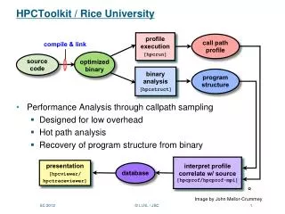
Download
1 / 39
410 likes | 599 Views
Carbon Nanotube Field-Effect Transistors (CNTFETs): Evolution and Applications for Future Nanoscale ICs. Tamer Ragheb ELEC 527 Presentation Rice University 3/15/2007. Conventional Semiconductor Microelectronics Will Come to an End. Vertical Scaling. Lateral Scaling.

E N D
Carbon Nanotube Field-Effect Transistors (CNTFETs): Evolution and Applications for Future Nanoscale ICs Tamer Ragheb ELEC 527 Presentation Rice University 3/15/2007
Conventional Semiconductor Microelectronics Will Come to an End Vertical Scaling Lateral Scaling • Conventional semiconductor device scaling obstacles: • Diffusion areas will no longer be separated by a low doped channel region • Equivalent gate oxide thickness will fall below the tunneling limit • Lithography costs will increase exponentially • Solution: • Find new technologies such as molecular electronics and CNT Hoenlein et al., Materials Science and Engineering: C, 2003
Why Carbon Nanotubes (CNTs)? • CNTs exhibit remarkable electronic and mechanical characteristics due to: • Extraordinary strength of the carbon-carbon bond • The small atomic diameter of the carbon atom • The availability of free π-electrons in the graphitic configuration Hoenlein et al., Materials Science and Engineering: C, vol. 23, no. 8, pp. 663-669, 2003
Carbon Nanotube Field-Effect Transistors (CNTFETs): Evolution • Most of the CNTFETs employ: • Semiconductor Single-walled carbon nanotube (SWCNT) as the channel • The contacts of SWCNT are the source and drain regions • A gate plate to control the conduction behavior of SWCNT • Tans et al. reported the first CNTFET (1998) • Used SWCNT as a channel • Platinum (Pt) as contacts • Silicon (Si) as a back-gate Tans et al., Nature, vol. 393, pp. 49-52, 1998 Hoenlein et al., Materials Science and Engineering: C, 2003
Carbon Nanotube Field-Effect Transistors (CNTFETs): Evolution • Tans at al.’s CNTFET exhibits p-type FET behavior • Tans et al. succeeded to modulate the conductivity over more than 5 orders of magnitude • The problem was the thick oxide layer used Tans et al., Nature, vol. 393, pp. 49-52, 1998
Carbon Nanotube Field-Effect Transistors (CNTFETs): Evolution n-type FET Enhanced-mode p-type FET • Bachthold et al. replaced: • The Si-back gate by a patterned Al-gate • The thick SiO2 layer by a thin Al2O3 layer • Platinum (Pt) contacts by gold (Au) • The gate biasing can change the behavior from p-type to n-type • Bachthold at al. succeeded to build different logic gates using the p-type behavior Bachthold et al., Science, vol. 294, pp. 49-52, 2001
Carbon Nanotube Field-Effect Transistors (CNTFETs): Evolution • Bachthold et al. simulated circuits: Bachthold et al., Science, vol. 294, pp. 49-52, 2001
Carbon Nanotube Field-Effect Transistors (CNTFETs): Evolution • Due to difficulty of back gate biasing, Wind et al. proposed the first CNTFET with top gate • The top gate is divided into 4 gate segments • Each segment is individually biased for more behavior control Wind et al., Physical Review Letters, vol. 91, no. 5, 2003
Carbon Nanotube Field-Effect Transistors (CNTFETs): Evolution • Top-gated CNTFETs allow: • Local gate biasing at low voltage • High speed switching • High integration density • Yang et al. compared the performance of: • Bottom-gate without top oxide • Bottom-gate with top oxide • Top-gate with top oxide • The top oxide used is TiO2 (high-k dielectric) Yang et al., Applied Physical Letters, vol. 88, p. 113507, 2006
Carbon Nanotube Field-Effect Transistors (CNTFETs): Evolution • Yang et al. proved that: • Top gate reduces the hysteresis behavior of CNTFET • Top gate reduces the needed gate voltage Yang et al., Applied Physical Letters, vol. 88, p. 113507, 2006
Carbon Nanotube Field-Effect Transistors (CNTFETs): Evolution • Derycke et al. proposed the first CMOS-like device by producing n-type CNTFETs by: • Annealing in a vacuum at 700K • Doping with potassium (K) • Derycke et al. succeeded to build the first CMOS-like inverter Derycke et al., Nano Letters, vol. 1, no. 9, pp. 453-456, 2001
Carbon Nanotube Field-Effect Transistors (CNTFETs): Evolution • The inverter fabrication steps: Derycke et al., Nano Letters, vol. 1, no. 9, pp. 453-456, 2001
Carbon Nanotube Field-Effect Transistors (CNTFETs): Evolution • Javey et al. proposed converting p-type into n-type by field manipulation • Javay et al. succeeded to build different logic gates Javey et al., Nano Letters, vol. 2, no. 9, pp. 929-932, 2002
Carbon Nanotube Field-Effect Transistors (CNTFETs): Evolution • Javey et al.’s circuits: Javey et al., Nano Letters, vol. 2, no. 9, pp. 929-932, 2002
Carbon Nanotube Field-Effect Transistors (CNTFETs): Evolution • Chen et al. proposed a complete integrated logic circuit assembled on a single CNT • They controlled the polarities of the FETs by using metals with different work functions as the gates Chen et al., Science, vol. 311, p. 1735, 2006
Carbon Nanotube Field-Effect Transistors (CNTFETs): Evolution Vdd=0.5V Vdd=0.92V • Chen et al.’s circuit is a voltage controlled (Vdd) ring oscillator Chen et al., Science, vol. 311, p. 1735, 2006
Carbon Nanotube Field-Effect Transistors (CNTFETs): Evolution • Hoenlein et al. proposed a vertical CNTFET (VCNTFET), it consists of: • 1nm diameter 10nm long SWCNT • A coaxial gate and a gate dielectric with 1nm thickness Hoenlein et al., Materials Science and Engineering: C, vol. 23, no. 8, pp. 663-669, 2003
Carbon Nanotube Field-Effect Transistors (CNTFETs): Evolution • VCNTFET has the advantages of: • Vertical growth in CNT is much easier and aligned than horizontal growth • 3D connections can be used in the vertical configuration Hoenlein et al., Materials Science and Engineering: C, vol. 23, no. 8, pp. 663-669, 2003
Carbon Nanotube Field-Effect Transistors (CNTFETs): Evolution • All the previous structures depend on semiconductor SWCNT. • SWCNT available commercially contain about 33-60% metallic CNTs. • For mass production and high yield, methods have to be found to guarantee that CNTFETs use semiconductor type SWCNTs. • Chen et al. and Na et al. proposed 2 different methods to convert metallic CNTs into semiconductor type. Chen et al., Japanese Journal of Applied Physics, vol. 45, no. 4B, pp. 3680-3685, 2006 Na et al., Fullerenes, Nanotubes, and Carbon Nanostructures, vol. 14, pp. 141-149, 2006
Carbon Nanotube Field-Effect Transistors (CNTFETs): Evolution • Chen et al. used plasma treatment to convert metallic CNT to semiconductor type. Chen et al., Japanese Journal of Applied Physics, vol. 45, no. 4B, pp. 3680-3685, 2006
Carbon Nanotube Field-Effect Transistors (CNTFETs): Evolution Measured values Theoretically • Na et al. used protein-coated nanoparticles in the contact areas to convert metallic CNT to semiconductor type. Na et al., Fullerenes, Nanotubes, and Carbon Nanostructures, vol. 14, pp. 141-149, 2006
Carbon Nanotube Field-Effect Transistors (CNTFETs): Evolution • Liang et al. proposed building CNTFET using a double-walled CNT (DWCNT) • The inner-shell is the gate due to its low conductance • The outer-shell is the channel due to its high conductance • It is easy to fabricate high-quality DWCNT • In fabrication: • Cover the outer-shell partially by polymer-patterns • The exposed part can be etched by H2O or O2 plasma at room temperature Pd contacts Router=1.73nm Rinner=1.39nm Inter-shell separation=0.34nm Liang et al., Physica. E, low-dimentional systems and nanostructures, vol. 23, no. 1-2, pp. 232-236, 2004
Carbon Nanotube Field-Effect Transistors (CNTFETs): Evolution • Liang et al.’s CNTFET simulation results: Liang et al., Physica. E, low-dimentional systems and nanostructures, vol. 23, no. 1-2, pp. 232-236, 2004
CNTFET as Memory Devices • Cui et al. employed CNTFET charge storage behavior to build a non-volatile memory • The memory device is stable to hold the data over a period of at least 12 days in the ambient conditions Cui et al., Applied Physics Letters, vol. 81, no. 17, pp. 3260-3262, 2002
CNTFET as Memory Devices • To avoid the probability of metallic CNT, Cui et al. used two methods: • Annealing (to heat at 335K for different periods) • Controlled oxygen plasma treatment at room temperature Cui et al., Applied Physics Letters, vol. 81, no. 17, pp. 3260-3262, 2002
CNTFET as Memory Devices • Lu et al. proposed a non-volatile flash memory device using: • CNTs as floating gates • HfAlO as control/tunneling oxide • Platinum (Pt) as top electrodes • CNT insertion enhances the memory behavior by holes trapping Lu et al., Applied Physics Letters, vol. 88, p. 113104, 2006
Short Channel CNTFET (Sub-20nm) • Seidel et al. proposed a fabrication method to obtain CNTFET with sub-20nm long channels Seidel et al., Nano Letters, vol. 5, no. 1, pp. 147-150, 2005
Single Electron CNTFET • Cui et al. fabricated single electron CNTFET (quantum dot) with a length of 10nm • The observed differential conductance peaks are a clear signature of single electron tunneling in the device Cui et al., Nano Letters, vol. 2, no. 2, pp. 117-120, 2002
Electro-Chemical CNTFET • Shimotani et al. studied another kind of CNTFET, which is electro-chemical CNTFET • In this transistor the gate is the electrolyte solution Shimotani et al., Applied Physics Letters, vol. 88, p. 073104, 2006
CNTFET as a Chemical Sensor • CNTFETs are very sensitive devices to chemicals. • Zhang et al. studied the sensing mechanism of CNTFET to NO2 and NH3 • CNT body is more sensitive to ammonia • CNT contacts are more sensitive to NO2 Zhang et al., Applied Physics Letters, vol. 88, p. 123112, 2006
CNTFET in RF Circuits • Zhang et al. measured the RF performance of CNTFETs RF Measurement circuitry Measurement results Zhang et al., IEEE Electron Device Letters, vol. 27, no. 8, pp. 668-670, 2006
CNTFET in RF Circuits • Zhang et al. proposed an RF simple model for CNTFET Zhang et al., IEEE Electron Device Letters, vol. 27, no. 8, pp. 668-670, 2006
CNTFET in RF Circuits • Pesetski et al. employed CNTFET to build RF circuits that can operate up to 23GHz Pesetski et al., Applied Physics Letters, vol. 88, p. 113103, 2006
CNTFET Built on Insulator • Liu et al. succeeded to build a novel nanotube-on-insulator (NOI) CNTFET similar to silicon-on-insulator (SOI) technology Liu et al., Nano Letters, vol. 6, no. 1, pp. 34-39, 2006
CNTFET Built on Insulator • Liu et al. built NOI transistors with: • Top-gated • Polymer-electrolyte-gated Liu et al., Nano Letters, vol. 6, no. 1, pp. 34-39, 2006
Conclusions • CNT is a future replacement for semiconductor based microelectronics • The evolution of CNTFET is discussed • Employing CNTFET in a lot of applications such as: • Logic circuits • Memories • Chemical sensors • RF circuits • Integrating CNT based interconnects with devices can produce a complete future nanoscale ICs
References (in Order of Appearance) • Hoenlein et al., Materials Science and Engineering: C, vol. 23, no. 8, pp. 663-669, 2003 • Tans et al., Nature, vol. 393, pp. 49-52, 1998 • Bachthold et al., Science, vol. 294, pp. 49-52, 2001 • Wind et al., Physical Review Letters, vol. 91, no. 5, 2003 • Yang et al., Applied Physical Letters, vol. 88, p. 113507, 2006 • Derycke et al., Nano Letters, vol. 1, no. 9, pp. 453-456, 2001 • Javey et al., Nano Letters, vol. 2, no. 9, pp. 929-932, 2002 • Chen et al., Science, vol. 311, p. 1735, 2006 • Chen et al., Japanese Journal of Applied Physics, vol. 45, no. 4B, pp. 3680-3685, 2006 • Na et al., Fullerenes, Nanotubes, and Carbon Nanostructures, vol. 14, pp. 141-149, 2006 • Liang et al., Physica. E, low-dimentional systems and nanostructures, vol. 23, no. 1-2, pp. 232-236, 2004 • Cui et al., Applied Physics Letters, vol. 81, no. 17, pp. 3260-3262, 2002 • Lu et al., Applied Physics Letters, vol. 88, p. 113104, 2006 • Seidel et al., Nano Letters, vol. 5, no. 1, pp. 147-150, 2005 • Cui et al., Nano Letters, vol. 2, no. 2, pp. 117-120, 2002 • Shimotani et al., Applied Physics Letters, vol. 88, p. 073104, 2006 • Zhang et al., Applied Physics Letters, vol. 88, p. 123112, 2006 • Pesetski et al., Applied Physics Letters, vol. 88, p. 113103, 2006 • Liu et al., Nano Letters, vol. 6, no. 1, pp. 34-39, 2006
Thank You Acknowledgments: Prof. James M. Tour and Prof. Lin Zhong Colleagues in RAND group Colleagues in the ELEC 527 class
Carbon Nanotube Field-Effect Transistors (CNTFETs): Evolution Not usable CNTs • Chen et al. used plasma treatment to convert metallic CNT to semiconductor type. Chen et al., Japanese Journal of Applied Physics, vol. 45, no. 4B, pp. 3680-3685, 2006