Download
1 / 32
320 likes | 399 Views
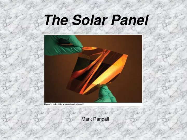
The Solar Panel. Mark Randall. History Everyone Else did it!!. 1839: Nineteen-year-old Edmund Becquerel, a French experimental physicist, discovered the photovoltaic effect while experimenting with an electrolytic cell made up of two metal electrodes. .

E N D
The Solar Panel Mark Randall
HistoryEveryone Else did it!! • 1839: Nineteen-year-old Edmund Becquerel, a French experimental physicist, discovered the photovoltaic effect while experimenting with an electrolytic cell made up of two metal electrodes. . • 1876: Adams and Day observed the photovoltaic effect in solid selenium. • 1883: Charles Fritts, an American inventor, described the first solar cells made from selenium wafers. • 1887: Heinrich Hertz discovered that ultraviolet light altered the lowest voltage capable of causing a spark to jump between two metal electrodes. • 1904: Hallwachs discovered that a combination of copper and cuprous oxide was photosensitive. Einstein published his paper on the photoelectric effect. • 1914: The existence of a barrier layer in PV devices was reported. • 1916: Millikan provided experimental proof of the photoelectric effect. • 1918: Polish scientist Czochralski developed a way to grow single-crystal silicon. • 1923:Albert Einstein received the Nobel Prize for his theories explaining the photoelectric effect. • 1951: A grown p-n junction enabled the production of a single-crystal cell of germanium. • 1954: The PV effect in Cd was reported; primary work was performed by Rappaport, Loferski and Jenny at RCA. Bell Labs researchers Pearson, Chapin, and Fuller reported their discovery of 4.5% efficient silicon solar cells; this was raised to 6% only a few months later (by a work team including Mort Prince). Chapin, Fuller, Pearson (AT&T) submitted their results to the Journal of Applied Physics. AT&T demonstrated solar cells in Murray Hill, New Jersey, then at the National Academy of Science Meeting in Washington, DC. • 1955: Western Electric began to sell commercial licenses for silicon PV technologies; early successful products included PV-powered dollar bill changers and devices that decoded computer punch cards and tape. Bell System's demonstration of the type P rural carrier system began in Americus, Georgia. Hoffman Electronics's Semiconductor Division announced a commercial PV product at 2% efficiency; priced at $25/cell and at 14 mW each, the cost of energy was $1500/W. • 1957: Hoffman Electronics achieved 8% efficient cells. "Solar Energy Converting Apparatus," patent #2,780,765, was issued to Chapin, Fuller, and Pearson, AT&T. • 1958: Hoffman Electronics achieved 9% efficient PV cells. Vanguard I, the first PV-powered satellite, was launched in cooperation with the U.S. Signal Corp. The satellite power system operated for 8 years.
More History • 1956: Bell System's demonstration of the type P rural carrier system was terminated after five months. • 1959: Hoffman Electronics achieved 10% efficient, commercially available PV cells and demonstrated the use of a grid contact to significantly reduce series resistance. Explorer-6 was launched with a PV array of 9600 cells, each only 1 cm x 2 cm. • 1960: Hoffman Electronics achieved 14% efficient PV cells. • 1961: The UN conference on Solar Energy in the Developing World was held. The precursor to the PV Specialists Conference, the Meeting of the Solar Working Group (SWG) of the Interservice Group for Flight Vehicle Power, was held in Philadelphia, Pennsylvania. The first PV Specialists Conference was held in Washington, DC. • 1963: Japan installed a 242-W PV array on a lighthouse, the world's largest array at that time. • 1964: The Nimbus spacecraft was launched with a 470-W PV array. • 1965: Peter Glaser, A.D. Little, conceived the idea of a satellite solar power station. Tyco Labs developed the edge-defined, film-fed growth (EFG) process, first to grow crystal sapphire ribbons and then silicon. • 1966: The Orbiting Astronomical Observatory was launched with a 1-kW PV array. • 1968: The OVI-13 satellite was launched with two CdS panels. • 1972: The French install a CdS PV system in a village school in Niger to run an educational TV. • 1973: The Cherry Hill Conference was held in Cherry Hill, New Jersey. • 1974: Japan formulated Project Sunshine. Tyco Labs grew the first EFG, 1-inch-wide ribbon by an endless-belt process. • 1975: The U.S. government began a terrestrial PV research and development project, assigned to the Jet Propulsion Laboratory (JPL), as a result of recommendations of the Cherry Hill Conference. Bill Yerkes opened Solar Technology International. Exxon opened Solar Power Corporation. JPL instituted the Block I procurement by the U.S. government. • 1977: The Solar Energy Research Institute (SERI), later to become the National Renewable Energy Laboratory (NREL), opened in Golden, Colorado. Total PV manufacturing production exceeded 500 kW.
More More History • 1979: Solenergy was founded. NASA's Lewis Research Center (LeRC) completed a 3.5-kW system on the Papago Indian Reservation in Schuchuli, Arizona; this was the world's first village PV system. NASA's LeRC completed an 1.8-kW array for AID, in Tangaye, Upper Volta, and later increased power output to 3.6 kW. • 1980: The first William R. Cherry Award was given to Paul Rappaport, SERI's founding director. New Mexico State University, Las Cruces, was selected to establish and operate the Southwest Residential Experimental Station (SW RES). A 105.6-kW system was dedicated at Natural Bridges National Monument in Utah; the system used Motorola, ARCO Solar, and Spectrolab PV modules. • 1981: A 90.4-kW PV system was dedicated at Lovington Square Shopping Center (New Mexico) using Solar Power Corp. modules. A 97.6-kW PV system was dedicated at Beverly High School in Beverly, Massachusetts, using Solar Power Corp. modules. An 8-kW PV-powered (Mobil Solar), reverse-osmosis desalination facility was dedicated in Jeddah, Saudi Arabia. • 1982: Worldwide PV production exceeded 9.3 MW. Solarex dedicated its 'PV Breeder' production facility in Frederick, Maryland, with its roof-integrated 200-kW array. ARCO Solar's Hisperia, California, 1-MW PV plant went on line with modules on 108 dual-axis trackers. • 1983: The JPL Block V procurement was begun. Solar Power Corporation completed the design and installation of four stand-alone PV village power systems in Hammam Biadha, Tunesia (a 29-kW village power system, a 1.5-kW residential system, and two 1.5-kW irrigation/pumping systems). Solar Design Associates completed the stand-alone, 4-kW (Mobil Solar), Hudson River Valley home. Worldwide PV production exceeded 21.3 MW, and sales exceeded $250 million. • 1984: The IEEE Morris N. Liebmann Award was presented to Drs. David Carlson and Christopher Wronski at the 17th Photovoltaic Specialists Conference, "for crucial contributions to the use of amorphous silicon in low-cost, high-performance photovoltaic solar cells." • 1991: The Solar Energy Research Institute was redesignated as the U.S. Department of Energy's National Renewable Energy Laboratory by President George Bush. • 1993: The National Renewable Energy Laboratory's Solar Energy Research Facility (SERF), opened in Golden, Colorado. • 1996: The U.S. Department of Energy announces the National Center for Photovoltaics, headquartered in Golden, Colorado.
The Solar Panel Makeup • 1 Cover Glass • 2 Antireflective coating • 3 Front Contact • 4 n-type Material • 5 P-type Material • 6 Back Contact The Solar Panel is Made up of 6Layers
What Types of Material Can be Used? • 1 Silicon • 2 Gallium Arsenide • 3. Polycrystalline Thin Films
Silicon Solar Cell Advantages • Silicon is easy to come by. • Relatively inexpensive Disadvantages • Silicon must be 99.9% Pure • Very inefficient
Silicon Solar Cell • Silcon may be used in 2 different forms 1. Single Crystal • More effitent transfer of electrons through Material • Hard/Costly to Grow 2. Semicrystalline • Very cheep to Manufacture • Has Grain Boundaries
Gallium Arsenide (GaAs) Compound Semiconductor Advantages • Molecular makeup • Ideal Band Gap • Very High Absorbability • Can be made very thin • Resistant to Radiation Disadvantages • Very Hard to come by • Gallium is Rarer than Gold • Arsenic is Poison
Gallium Arsenide (GaAs) Compound Semiconductor • The cell can have several layers of slightly different compositions that allow a cell designer to precisely control the generation and collection of electrons and holes. • This degree of control allows cell designers to push efficiencies closer and closer to theoretical levels (30%)
Polycrystalline Thin Films Advantages • Take very little semiconductor material • Easy to manufacture • Large or small cells • Made into virtually any shape Disadvantages • ???? • Very new technology
Polycrystalline Thin Films • Unlike most single-crystal cells, the typical thin film device does not use a metal grid for the top electrical contact. Instead it uses a thin layer of transparent conducting oxide. • These oxides are highly transparent and conduct electricity very well. A separate antireflection coating may be used to top of the device, or the transparent conducting oxide may serve this function as well. This helps to bring the manufacturing cost even lower.
THE BAND GAP Damn Buzz Words
THE BAND GAP In solid state physics and related applied fields, the band gap is the energy difference between the top of the valence band and the bottom of the conduction band in insulators and semiconductors. It is often spelt "bandgap".
THE BAND GAP • Each Type of Material has its own band gap • The band gap determines how much energy a photon must have to remove a electron from the valence band of the atom • Silicon has a band gap of 1.14 eV and 0.77 eV
THE BAND GAP • The band gap works basically like a band pass filter (photons with small amounts of energy will not remove electrons and photons with large amount of energy will not remove electrons) • Therefore most Silicon Solar Cells are “Tuned” for infrared or Red Light • This is one of the many reasons that per unit area Solar Cells are so inefficient
THE BAND GAP • Newer technologies are allowing single cells to have several band gaps this allows the cell to use more of the light spectra. • ENOUGH ABOUT THE BAND GAP!!!!!
New Technologies: • Organic solar cells • Dye-sensitized solar cells • Nanotechnology solar cells • "Third-generation" solar cells About half the cost of a PV system is due to the PV module itself. Presently, through two programs—Beyond-the-Horizon PV and Future-Generation PV—we are examining four new approaches to solar cells that promise—in the long term—to dramatically reduce the cost of this component in PV systems:
Organic and Dye Solar Cells • Dye and organic solar cells represent a recently developed class of solar cells, which is based on completely different principles to semiconductor technology. The basis for production is inexpensive thin-film technology, such as is already applied in industrial processing of glass and polymers. This offers the potential for financially attractive manufacturing. Properties such as transparency and color for the dye cells, and mechanical Flexibility for the polymer-based solar cells, can be adapted as needed for specific products, opening up completely new application areas for photovoltaics
An unexpected discovery • BERKELEY, CA — Researchers in the Materials Sciences Division (MSD) of Lawrence Berkeley National Laboratory, working with crystal-growing teams at Cornell University and Japan's Ritsumeikan University, have learned that the band gap of the semiconductor indium nitride is not 2 electron volts (2 eV) as previously thought, but instead is a much lower 0.7 eV.
An unexpected discovery • The serendipitous discovery means that a single system of alloys incorporating indium, gallium, and nitrogen can convert virtually the full spectrum of sunlight -- from the near infrared to the far ultraviolet -- to electrical current. • if solar cells can be made with this alloy, they promise to be rugged, relatively inexpensive -- and the most efficient ever created.
The Search For Better Efficiency Limiting Factors • Silicon wastes most energy as heat • Band Gap limitations • Low absorption rates
The Search For Better Efficiency • Maximum efficiency is about 30% • (for single material solar cell) • Best efficiency actually achieved is 25% • (for single material solar cell) • To increase efficiency different band gap material are stacked to form multijunction cells • These cells have much higher efficiency • But are much more expensive to manufacture