Download
1 / 17
170 likes | 373 Views
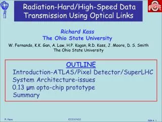
Rad -Hard ASICS for Optical Data Transmission in the 1 st Phase of the LHC Upgrade. A. Adair, W. Fernando, K.K. Gan, H.P. Kagan, R.D. Kass, H. Merritt, J. Moore, A. Nagarkar, S. Smith, M. Strang The Ohio State University. P. Buchholz, A. Wiese, M. Ziolkowski Universität Siegen. OUTLINE

E N D
Rad-Hard ASICS for Optical Data Transmission in the 1st Phase of the LHC Upgrade A. Adair, W. Fernando, K.K. Gan, H.P. Kagan, R.D. Kass, H. Merritt, J. Moore, A. Nagarkar, S. Smith, M. Strang The Ohio State University P. Buchholz, A. Wiese, M. Ziolkowski Universität Siegen OUTLINE Introduction Result on PIN Receiver/Decoder Chip Result on VCSEL Driver Chip Summary
ATLAS Insertable B Layer ~1.85m Proposal to add one more layer to the current pixel detector: Insertable B-Layer or IBL Installation ~ 2015-6 Optical readout will use VCSEL/PIN array Propose to use an updated version of current driver (VDC) & receiver/decoder (DORIC) chips Upgrades include redundancy & individual VCSEL current control Valuable experience for development of SLHC system Experience gained from the development/testing of such new chips would help the development of on-detector array-based opto-links for SLHC Will discuss results from 1st prototype chip (130 nm) submitted 2/2010, received 6/2010, beam test 8/2010
Chip Content VCSEL:Vertical Cavity Surface Emitting Laser diode VDC:VCSEL Driver Circuit PIN:PiNdiode DORIC:Digital Optical Receiver Integrated Circuit The DORIC decodes bi-phase mark encoded clock & commands Design Photo VCSEL Driver (spare) VCSEL Driver VCSEL Driver with pre-emphasis VCSEL Driver with pre-emphasis CML Driver with pre-emphasis Decoder (40Mb/s) Decoder (40Mb/s) Decoder (40Mb/s) Decoder (40/80/160/320 Mb/s, spare) 1.5 mm
PIN Receiver/Decoder PIN Prototype chip only.
Command Decoder Interface Courtesy of FE-I4 of IBL Prototype: majority voting, 3 command decoders Production: majority voting, up to 11 command decoders In prototype chip only
Decoder Test Card Test card PIN opto-pack ULM 5 Gb/s chip
Recovered Clock/Data Decoder recovers clock & data from bi-phase mark input stream Decoded clock 320 Mb/s Decoded data
PIN Receiver/Decoder Measured Jitter & Threshold Threshold for no bit errors: 40 Mb/s: Multi speed: 40 mA Ch 1: 19 mA Ch 2: 22 mA Ch 3: 20 mA 80 Mb/s: 58 mA 160 Mb/s: 74 mA 320 Mb/s: 110 mA Peak-to-peak clock jitter: 40 Mb/s: 1420 ps (multi speed) 80 Mb/s: 750 ps 160 Mb/s: 193 ps 320 Mb/s: 103 ps All channels work at 40 Mb/s Multi Speed version works at 40, 80, 160, & 320 Mb/s 160 & 320 Mb/s need external bias tuning for proper operation Steering signal to the spare channel works
VCSEL Driver Section Set DAC Command Write DAC Bits (7:0) Channel Select (3:0) Write Enable (3:0) VCSEL input added for prototype chip only.
VDC Test Setup Light from the 4 VCSELs Fiber aligned over VDC/VCSEL 2 Finisar 5 Gb/s VCSEL array Opto-chip
VDC Results Power-on reset circuit In the present pixel detector an open control line disables 6 opto-links Prototype chip has a power-on reset circuit chips will power up with several mA of VCSEL current Test port can steer signal received to spare VDC/VCSEL can set DAC to control individual VCSEL currents All 4 channels run error free at 5 Gb/s includes the spare with signal routed from the other inputs
VCSEL Driver with Pre-Emphasis 160 Mb/s Main amplitude Pre-emphasis Pre-emphasis working with tunable width and height
Eye Diagrams @ 4.8 Gb/s Spare VDC: rerouted from VDC 2 VDC 3 No pre-emphasis Rise/fall times: ~60-90 ps Measured with 4.5 GHz optical probe Bit error rate < 5x10-13
Irradiation Results 2 chips were packaged for irradiation with 24 GeV/c protons at CERN in August 2010 Each chip contains 4 channels of drivers and receivers Total dose: 1.6 x 10¹⁵ protons/cm2 All tests are electrical to avoid complications from degradation of optical components Long cables limited testing to low speed Observe little degradation of the devices Evaluation of full performance await the return of devices to OSU from CERN
VDC Irradiation Results 2010 2008 VDC driving 25 Ω with constantcontrol current (CC) Previous VDC prototypes (130 nm) irradiated in 2008 Drive current decreases with radiation for constant CC driver circuit fabricated with thick oxide process PMOS and NMOS have different threshold voltage shifts Use only PMOS in the current mirror in 2010 prototype See improvement in the 2010 version
Single Event Upset Rate SEU hardend latches or DAC could be upset by traversing charged particles 126 latches per 4-channel chip SEU tracked by monitoring the amplitude of the VDC drive current 13 instances (errors) of a channel steered to a wrong channel in 71 hours for chip #1 Similar upset rate in chip #2 Estimate SEU rate: σ = 1x10-16 cm2 particle flux ~3x109 cm-2/year @ opto-link location SEU rate ~3x10⁻⁷/year/link
Summary Prototyped opto-chip for 2nd generation ATLAS pixel opto-links Incorporated experience from current opto-links by adding: redundancy to bypass broken PIN or VCSEL channel individual VCSEL current control power-on reset to set VCSEL current to several mA upon power up Results of tests: VCSEL driver can operate up to ~ 5 Gb/s with BER < 5x10-13 PIN receiver/decoder works even at low threshold Only small decrease in VDC output current after irradiation Very low SEU rate in latches/DAC All added functionalities work! All results are preliminary