Download
1 / 17
170 likes | 271 Views
Processor implementation on Altera DE2 Development and Education Board. V. Mitić, M. Petković, D. Todorović 1 , Volker Zerbe 2. 1 - University of Nis, Faculty of Electronic Engineering ; 2 - University of Applied Sciences, Erfurt. Agenda. Introducing to: Hardware

E N D
Processor implementation on Altera DE2 Development and Education Board V. Mitić, M. Petković, D. Todorović 1, Volker Zerbe 2 1 - University of Nis, Faculty of Electronic Engineering; 2 - University of Applied Sciences, Erfurt
Agenda • Introducing to: • Hardware • Altera Developement and Education Boards • FPGAs • Software • Programming tools for FPGAs • VHDL
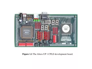
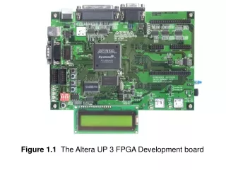
Introduction • Technology • Altera Quartus II • DE2 Development and Education Board
Design, fabrication and code • Processor Block Diagram/Schematic file • Operations symbols • 8bitadder, 8bitsupstract, 8bitand, 8bitor, 8bitnot, 8bitxor, 8bitnand, 8bitnor • Multiplexer symbols • Multiplexernot, Multiplexer, Multiplexer2, Multiplexerrez • HEXdec symbol • Converter symbol
HEXdec Input numbers Operations Multiplexers Output Displays Input pushbuttons Output LEDs Input selector switches Processor Block Diagram/Schematic file
Operations symbols • 8bitadderAddition is done with the useof two symbols:halfadder and fullader.
HALFADDER FULLADDER
Multiplexernot • There are two 8-bit numbers on the input and two selector pins (SEL0-SEL1) • There is one 8-bit number on the output. • The output number is eaqual to one of the input numbers depending of the selector pins.
HEXdec symbol • This symbol performs conversion of a binary number, which is at the input, into a decimal number which is displayed on the 7- segment displays. • There are 9 input and 49 output pins. • The conversion from binary to decimal numeral system is implemented using converter symbol. • Representation of a number onto 7-segment display is done with symbols HEX0-HEX9.
Converter symbol • This symbol is a graphical representation of converter.vhd file that is written in VHDL code. • This symbol does not only convert the number, but also it “determines” the distribution of digits in the decimal number. • There are 9 input pins and 29 output pins. • All commands are executed in a process (named CONVERSION) because they have to be executed sequentially (one by one).
Results in brief • Aquired knowlage about: • Elements and posibilities of DE2 Development and Education Board • Basics of VHDL (via converter.vhd) • Altera Quartus tools for synthesis and simulation • FPGAs
Conclusion • DE2 Developement and Education board advantages • FPGA advantages • VHDL advantages • Implementation: from lab demos to ESA projects
Thank you for your attention! Any questions?