Download
1 / 70
730 likes | 1.01k Views
SDR ham, A Software Defined Radio Project Nordic VHF/UHF/SHF Meeting 2007. SDR FE. USB. The Project. Project started in 2004 Project goals Develop an SDR FE (Front End) hardware Develop SDR PC software Learn SDR technology Learn Digital Signal Processing

E N D
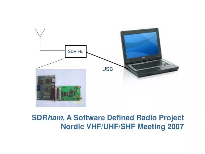
SDRham, A Software Defined Radio ProjectNordic VHF/UHF/SHF Meeting 2007 SDR FE USB
The Project • Project started in 2004 • Project goals • Develop an SDR FE (Front End) hardware • Develop SDR PC software • Learn SDR technology • Learn Digital Signal Processing • Use SDR in amateur radio applications where high performance is needed • Weak signal reception in crowded HF bands • EME (Earth-Moon-Earth) communication in the VHF band • To have a plattform, SDR FE and PC, for development of analog and digital modes
Status May 2007 • First SDR FE running • A Windows/PC test application with SSB/CW demodulator is developed • Some initial performance testing is done
Participants • LA9CY, Kjell Syverud • LA7OU, Stein Erik Ellevseth • LA8TO, Odd Arild Olsen • LB8X, Tom Twist • LA7BO, Halvor Liland
Agenda • An introduction to SDRham • Applied technology and theory • Sampling • Filter design, time and frequency domain • USB, sample streaming • Signal Processing on PC • MMX and SSE instruction sets in Pentium CPU • Demodulation techniques • Tools • Receiver design
The Analog Devices Integrated Circuits AD6645 14-Bit, 80 MSPS AD Converter AD6620 Digital Receive Signal Processor
Technology and Tools • Tools • Borland C++ Builder6 • PC SDR SW • Keil µVision2 • EZ USB FX2 8051 code • Cypress EZ-USB Control Panel • USB communication • Altera Quartus II • EPLD • MathCAD • Filter design, analyses and simulation • Ansoft Harmonica • Analog Simulation • Technology • Direct RF sampling • to 200 MHz • USB • Digital Signal Processing on PC • MMX and SSE instruction set
ADC Module Design of KD7O
Analog to Digital Converter, AD6645 14-bit 80 MSPS ADC2 ADC3 ADC1 80 MSPS Guaranteed Sample Rate SNR = 75 dB, fIN 15 MHz @ 80 MSPS SNR = 72 dB, fIN 200 MHz @ 80 MSPS SFDR = 89 dBc, fIN 70 MHz @ 80 MSPS The AD6645 employs a three stage subrange architecture
Subranging ADC N-bit Two-Stage Subranging ADC
Missing Codes Missing Codes Due to MSB SADC Nonlinearity or Interstage Misalignment
SNR, SFDR and Process Gain (Measured over the Nyquist Bandwidth: DC to fS/2) Calculated SNR for an 14-bit ADC SFDR Process Gain fs = 64 MHz, BW = 3.2 kHz
Some “Magic” of Process Gain The AD6645 Input Voltage Range is 2.2 Vp-p.The voltage for LSB (Least Significant Bit) is then The voltage is then (134 uV) = 1 uVPEAK How can the ADC detect voltage levels of one hundred (-40 dB) of its LSB? Answer: The signal voltage is added to the ADC internal noise voltage, which is more than many LSBs. With a process gain of 40 dB the the signal will appear again. The power P in a signal of -110 dBm is found from
Sampling, Nyquist Zones Undersampling and Frequency Translation between Nyquist Zones A restate of the Nyquist criteria: A signal must be sampled at a rate equal to or greater than twice its bandwidth in order to preserve all the signal information The process of sampling a signal outside the first Nyquist zone is often referred to as undersampling or harmonic sampling
Mathematics of Undersampling A MathCad simulation proves theory
Noise Factor (NF) of the AD6645 NF is an important parameter in receivers. To calculate a receiver NF one need to know the NF of each stage. NF is normally not specified by ADC manufacturers.
Maximum Input Signal to the AD6645 A 1:4 impedance transformer makes the 50 ohm antenna input to 200 ohm at the AD6645 input. The maximum input voltage of the AD6645 is 2.2 VP-P, that is 0.78 VRMS. The power is then
Effect of Dither (MathCAD Simulation) With dither (normal distributed noise) Without dither
Digital Signal Receive Processor, AD6620 The AD6620 decimating receiver is designed to bridge the gap between high-speed ADCs and general purpose DSPs. It has four cascaded signal processing elements: a frequency translator, two fixed coefficient decimating filters and a programmable coefficient decimating filter.
Numeric Controlled Oscillator, NCO Frequency is phase change pr time interval. A phase change of 2л (360°) in 1 second is equal to a frequency of 1 Hz NCO_FREQ is interpreted as a 32-bit unsigned integer. NCO_FREQ is calculated by Clk = 16 MHz Phase increment = 1 -> f = 1 MHz Phase increment = 2 -> f = 2 MHz
Time and Frequency Domain Frequency Domain Time Domain Fourier transform og Fourier Series transform a signal between the time and frequency domain
The ideal filter in the frequency and time domain Ideal filter Ideal Low Pass Filter time domain response
Filter, frequency domain vs time domain Multiplication in the frequency domain is convolution in the time domain The Convolution Integral Changing variable with u = t - t and replace the integrals gives
FIR (Finite Impulse Response) Filter A finite impulse response (FIR) filter is a discrete linear time-invariant system whose output is based on the weighted summation of a finite number of past inputs. In the discrete domain (a sampled digital data system) the convolution integral changes to a summation
Cascaded Integrator Comb Filter, CIC The CIC filter is a fixed-coefficient, multiplierless, decimating filter. The characteristics are defined by the decimation rate.
CIC2 Frequency Response fSAMP = 65 MHz, MCIC2 = 10 BW = 4 kHz -> DR = 127 dB BW = 100 kHz -> DR = 71 dB
AD6620 RCF (RAM Coefficient Filter) The length of the filter kernel limits the transition bandwidth Where BW is a fraction of sampling frequency This filter is an FIR (Finite Impulse Response) filter
AD6620 Setup File, ad6620.imp MCIC2 MCIC5 MRCF fSAMP CHIP MODE CLK MULT FILTER COEFF 16 25 20 64000000 1 1 0 1 4 10 19 30 44 61 80 100 121 141 158 172 181 183 175 Low Pass Filter with 3 kHz cut off frequency
AD6620 Setup Dialog Box The dialog box reads parameters from a file or let the user change them
EPLD, Serial to Parallel Converter In the SDRham the serial output format of the AD6620 is used to get 24-bit resolution. An EPLD, Altera EPM3064, is used to convert the serial bit stream to the 8-bit parallel FIFO interface of the EZ USB FX2
Why 24-bit when the Input is 14-bit ? A sine wave sampled with 2-bit A sine wave sampled with 4-bit A sine wave sampled with 8-bit
EZ-USB FX2 The Cypress Semiconductor EZ-USB FX2 (often abbreviated as “FX2” ) is a single chip USB 2.0 peripheral with an 8051 microcontroller core
USB Transfer Types • Bulk Transfers • Bulk data is bursty, traveling in packets of 8, 16, 32 or 64 bytes at full speed or 512 bytes at high speed. Bulk data has guaranteed accuracy, due to an automatic retry mechanism for erroneous data. The host schedules bulk packets when there is available bus time. Bulk transfers are typically used for printer, scanner, or modem data. Bulk data has built-in flow control provided by handshake packets. • Interrupt Transfers • Interrupt data is like bulk data; it can have packet sizes of 1 through 64 bytes at full speed or up to 1024 bytes at high speed. Interrupt endpoints have an associated polling interval that ensures they will be polled (receive an IN token) by the host on a regular basis. • Isochronous Transfers • Isochronous data is time-critical and used to stream data like audio and video. An isochronous packet may contain up to 1023 bytes at full speed, or up to 1024 bytes at high speed.
Pipes and Endpoints The FX2 Full-Speed Alternate Settings From the driver point of view, the endpoints are referenced as pipes
USB used in the SDRham An OUT bulk endpoint is used for control (AD6620 setup) An IN isosynchronous endpoint is used for sample streaming
FX2 ReNumeration Once the Default USB Device enumerates, it downloads firmware and descriptor tables from the host into the FX2’s on-chip RAM. The FX2 then begins executing the downloaded code, which electrically simulates a physical disconnect/connect from the USB and causes the FX2 to enumerate again as a second device, this time taking on the USB personality defined by the downloaded code and descriptors. This patented secondary enumeration process is called “ReNumeration™.”
FX2 Access from Windows The FX2 is accessed through Windows API functions and a Cypress supplied driver ezusb.sys
MMX Instruction Set • The MMX instructions defines a SIMD (Single Instruction Multiple Data) model to handle 64-bit packed integer data. MMX adds the following new features to the Intel IA-32 architecture: • Eight new 64-bit MMX registers (aliased in th x87 register stack) • Three new packed data types • 64-bit packed byte integers (signed and unsigned) • 64-bit packed word integers (signed and unsigned) • 64-bit packed double word integers (signed and unsigned) • New instructions to support the new data types and to handle the MMX state management
MMX Execution Model and Instructions • MMX Instructions • Data Transfer • Arithmetic • Comparison • Unpacking • Logical • Shift • Empty MMX State Instruction
MMX Convolution Routine //--------------------------------------------------------------------------- void DSP001::MMXConvolute(int *src_ptr,int *dest_ptr,unsigned int size) { int dummy[]={0,0}; int *end_of_buffer=&psig_buf[(size_filter<<1)-2]; int *pbuf_sig=psig_buf; int *pbuf_filt=pfilt_buf; int *pbuf_signal=psignal_buf; unsigned int filtersize=size_filter; asm { MOV ECX,size TEST ECX,-1 JZ no_convolute //here to perform convolution MOV EBX,pbuf_signal //EBX is pointer to data line MOV ESI,src_ptr //ESI is pointer to source data MOV EDI,dest_ptr //EDI is pointer to destination data next_conv: filter_loop: MOVQ MM0,QWORD PTR [EBX] PSRAD MM0,8 //shift sourec to 16-bit PMULHW MM0,QWORD PTR [EDI] PADDSW MM1,MM0 //accumulated vale is in MM1 CMP EBX,end_of_buffer JGE new_start_buffer ADD EBX,8 JMP next_loop new_start_buffer: MOV EBX,pbuf_sig
SSE Instruction Set • The SSE (Streaming SIMD Extensions) add the following features to the IA-32 architecture • Eight 128-bit data registers, called XMM registers • 128-bit packed single-precision floating point data type (four IEEE single-precision floating point values packed into a double quad word) • Instructions that perform SIMD operations on single-precision floating point values and that extend the SIMD operations that can be performed on integers: • 128-bit packed and scalar single-precision floating point instructions that operate on data located in the XMM registers • 64-bit SIMD integer instructions that support additional operations on packled integer operands located in MMX registers • The SSE extensions were introduced in the Pentium III processor family
Demodulation Techniques Give me In-Phase (I) and Quadrature (Q) signal components, and you can get everything. The I- and Q-components contain both amplitude and phase information of a received signal. Frequency is found from phase change per time interval.
SSB Demodulation The phasing method To obtain a filter with 90o phase shift over many octaves is not so easy in the analog world. This is not a problem in a digital world (FIR filter)