SEQ CPU Implementation
580 likes | 708 Views
This documentation outlines the implementation stages of a sequential CPU design, focusing on the various hardware blocks and control logic necessary for executing instructions. It covers critical components such as ALUs, memory operations, fetch logic, decode processes, and write-back mechanisms. The sequential stages involve fetching instructions from memory, decoding them, executing operations through ALUs, and writing results back. Suggested reading sections improve understanding of concepts, providing a comprehensive guide for those studying CPU architecture and its implications in computer engineering.

SEQ CPU Implementation
E N D
Presentation Transcript
Outline • SEQ Stage Implementation • Suggested Reading 4.3.4
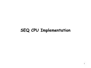
Data memory ALU Data srcA srcB srcA srcB PC increment valP PC PC newPC New PC data out valM read Memory Mem Control write Addr Bch valE Execute ALU fun CC ALUA ALUB valA valB dstE dstM Decode dstE dstM A B M Register file E Write Back icode ifun rA rB valC Instruction Memory Fetch 3
SEQ Hardware • Blue boxes: predesigned hardware blocks • e.g., memories, ALU • Gray boxes: control logic • Describe in HCL • White ovals: labels for signals • Thick lines: 32-bit word values • Thin lines: 4-8 bit values • Dotted lines: 1-bit values
Fetch Logic • Predefined Blocks • PC: Register containing PC • Instruction memory: Read 6 bytes (PC to PC+5) • Split: Divide instruction byte into icode and ifun • Align: Get fields for rA, rB, and valC
Fetch Logic • Control Blocks • Instr. Valid: Is this instruction valid? • Need regids: Does this instruction have a register bytes? • Need valC: Does this instruction have a constant word? • icode|ifun: Set to “nop” if imem_error
nop nop nop 0 0 0 0 0 0 0 0 halt halt halt 1 1 1 1 0 0 0 0 rA rA rA rB rB rB rA rA rA rA rB rB rB rB 2 2 2 2 0 0 0 0 rrmovl rrmovl rrmovl , , , V V V rB rB rB rB rB rB rB V V V 3 3 3 3 0 0 0 0 8 8 8 8 irmovl irmovl irmovl , , , rA rA rA D D D rB rB rB rA rA rA rA rB rB rB rB D D D 4 4 4 4 0 0 0 0 rmmovl rmmovl rmmovl , , , ( ( ( ) ) ) D D D rB rB rB rA rA rA rA rA rA rA rB rB rB rB D D D 5 5 5 5 0 0 0 0 mrmovl mrmovl mrmovl ( ( ( ), ), ), rA rA rA rB rB rB fn fn fn fn rA rA rA rA rB rB rB rB 6 6 6 6 OPl OPl OPl , , , Dest Dest Dest fn fn fn fn Dest Dest Dest 7 7 7 7 jXX jXX jXX Dest Dest Dest Dest Dest Dest 8 8 8 8 0 0 0 0 call call call ret ret ret 9 9 9 9 0 0 0 0 rA rA rA rA rA rA rA A A A A 0 0 0 0 8 8 8 8 pushl pushl pushl rA rA rA rA rA rA rA B B B B 0 0 0 0 8 8 8 8 popl popl popl need_regids
Fetch Control Logic bool need_regids = icode in { IRRMOVL, IIRMOVL, IRMMOVL, IMRMOVL, IOPL, IPUSHL, IPOPL }; bool instr_valid = icode in { INOP, IHALT, IRRMOVL, IIRMOVL, IRMMOVL, IMRMOVL, IOPL, IJXX, ICALL, IRET, IPUSHL, IPOPL };
Decode & Write Back Logic • Predefined Blocks • Registers File • Read ports A, B & Write ports E, M • Addresses are register IDs or F (no access)
Decode & Write Back Logic • Control Logic • srcA: read port address for valA {rA, %esp} • srcB: read port address for valB {rB, %esp} • dstE: write port address for valE {rB, %esp} • dstM: write port address for valM {rA} • Cnd: used to decide whether set valE (cmovXX)
A Source opl rA, rB Decode valA R[rA] Read operand A rmmovl rA, D(rB) Decode valA R[rA] Read operand A popl rA Decode valA R[%esp] Read stack pointer jXX Dest Decode No operand call Dest Decode No operand ret Decode valA R[%esp] Read stack pointer
A Source int srcA = [ icode in { IRRMOVL, IRMMOVL, IOPL, IPUSHL } : rA; icode in { IPOPL, IRET } : RESP; 1 : RNONE; # Don't need register ];
E Destination opl rA, rB Write-back R[rB] valE Write back result rmmovl rA, D(rB) Write-back None popl rA Write-back R[%esp] valE Update stack pointer jXX Dest Write-back None call Dest Write-back R[%esp] valE Update stack pointer ret Write-back R[%esp] valE Update stack pointer
E Destination int dstE = [ icode in { IRRMOVL, IIRMOVL, IOPL} : rB; icode in { IPUSHL, IPOPL, ICALL, IRET }: RESP; 1 : RNONE; # Don't need register ]; // cmovXX is not considered
Execute Logic • Predefined Blocks • ALU: implements 4 required functions and generate condition code values • CC: register with 3 condition code bits • cond: computes condition flag
Execute Logic • Control Logical • Set CC: Should condition code register be loaded? • ALU A: Input A to ALU {valA, valC, +4, -4} • ALU B: Input B to ALU {valB, 0} • ALU fun: What function should ALU compute?
ALU A Input OPl rA, rB Execute valE valB OP valA Perform ALU operation rmmovl rA, D(rB) Execute valE valB + valC Compute effective address popl rA Execute valE valB + 4 Increment stack pointer jXX Dest Execute No operation call Dest Execute valE valB + –4 Decrement stack pointer ret Execute valE valB + 4 Increment stack pointer
ALU A Input int aluA = [ icode in { IRRMOVL, IOPL } : valA; icode in { IIRMOVL, IRMMOVL,IMRMOVL} : valC; icode in { ICALL, IPUSHL } : -4; icode in { IRET, IPOPL } : 4; # Other instructions don't need ALU ];
ALU Operation opl rA, rB Execute valE valB OP valA Perform ALU operation rmmovl rA, D(rB) Execute valE valB + valC Compute effective address popl rA Execute valE valB + 4 Increment stack pointer jXX Dest Execute No operation call Dest Execute valE valB + –4 Decrement stack pointer ret Execute valE valB + 4 Increment stack pointer
ALU Operation / Condition Set int alufun = [ icode == IOPL : ifun; 1 : ALUADD; ]; Bool set_cc = icode in { IOPL };
Memory Logic • Predefined Blocks • Memory: Reads or writes memory word
Memory Logic • Control Logical • Mem. read: should word be read? • Mem. write: should word be written? • Mem. addr.: Select address {valA, valE} • Mem. data.: Select data {valA, valP}
Memory Memory Memory Memory valM M4[valA] M4[valE] valP M4[valE] valA valM M4[valA] Write return value on stack Read from stack Write value to memory Read return address Memory Address opl rA, rB Memory No operation rmmovl rA, D(rB) popl rA jXX Dest Memory No operation call Dest ret
Memory Address int mem_addr = [ icode in { IRMMOVL, IPUSHL, ICALL, IMRMOVL } : valE; icode in { IPOPL, IRET } : valA; # Other instructions don't need address ];
Memory Memory Memory Memory valM M4[valA] M4[valE] valP M4[valE] valA valM M4[valA] Write return value on stack Read from stack Write value to memory Read return address Memory Read opl rA, rB Memory No operation rmmovl rA, D(rB) popl rA jXX Dest Memory No operation call Dest ret
Memory Read/Write bool mem_read = icode in { IMRMOVL, IPOPL, IRET }; bool mem_write = icode in { IRMMOVL, IPUSHL, ICALL };
PC Update Logic • New PC • Select next value of PC
PC update PC update PC update PC update PC update PC update PC valM PC valC PC valP PC Bch ? valC : valP PC valP PC valP Update PC Update PC Set PC to return address Update PC Set PC to destination Update PC PC Update OPl rA, rB rmmovl rA, D(rB) popl rA jXX Dest call Dest ret
PC Update int new_pc = [ icode == ICALL : valC; icode == IJXX && Cnd : valC; icode == IRET : valM; 1 : valP; ];
SEQ Summary • Implementation • Express every instruction as series of simple steps • Follow same general flow for each instruction type • Assemble registers, memories, predesigned combinational blocks • Connect with control logic
Limitations of SEQ • Too slow to be practical • Too many tasks needed to finish in one clock cycle • instruction memory, register file, ALU, and data memory • Signals need long time to propagate through all of the stages • The clock must run slowly enough • Does not make good use of hardware units • Every unit is active for part of the total clock cycle
Outline • General Principles of Pipelining • Goal • Difficulties • Suggested Reading 4.4
Idea Divide process into independent stages Move objects through stages in sequence At any given times, multiple objects being processed Parallel Sequential Pipelined Real-World Pipelines: Car Washes
300 ps 20 ps Combinational logic R e g Delay = 320 ps Throughput = 3.12 GOPS Clock Computational Example • System • Computation requires total of 300 picoseconds • Additional 20 picoseconds to save result in register • Can must have clock cycle of at least 320 ps
100 ps 20 ps 100 ps 20 ps 100 ps 20 ps Comb. logic A R e g Comb. logic B R e g Comb. logic C R e g Delay = 360 ps Throughput = 8.33 GOPS Clock 3-Way Pipelined Version • System • Divide combinational logic into 3 blocks of 100 ps each • Can begin new operation as soon as previous one passes through stage A. • Begin new operation every 120 ps • Overall latency increases • 360 ps from start to finish
OP1 A A A B B B C C C OP2 OP3 OP1 Time OP2 Time OP3 Pipeline Diagrams • Unpipelined • Cannot start new operation until previous one completes • 3-Way Pipelined • Up to 3 operations in process simultaneously
50 ps 20 ps 150 ps 20 ps 100 ps 20 ps Comb. logic A R e g Comb. logic B R e g Comb. logic C R e g Delay = 510 ps Throughput = 5.88 GOPS Clock OP1 A A A B B B C C C OP2 OP3 Time Limitations: Nonuniform Delays
Limitations: Nonuniform Delays • Throughput limited by slowest stage • Other stages sit idle for much of the time • Challenging to partition system into balanced stages
Delay = 420 ps, Throughput = 14.29 GOPS 50 ps 20 ps 50 ps 20 ps 50 ps 20 ps 50 ps 20 ps 50 ps 20 ps 50 ps 20 ps Comb. logic R e g Comb. logic R e g Comb. logic R e g Comb. logic R e g Comb. logic R e g Comb. logic R e g Clock Limitations: Register Overhead
Limitations: Register Overhead • As try to deepen pipeline, overhead of loading registers becomes more significant • Percentage of clock cycle spent loading register: • 1-stage pipeline: 6.25% • 3-stage pipeline: 16.67% • 6-stage pipeline: 28.57% • High speeds of modern processor designs obtained through very deep pipelining
R e g Combinational logic Clock OP1 OP2 OP3 Time Data Dependencies • System • Each operation depends on result from preceding one
A A A A B B B B C C C C Comb. logic A R e g Comb. logic B R e g Comb. logic C R e g OP1 OP2 OP3 OP4 Time Clock Data Hazards