Download
1 / 11
110 likes | 208 Views
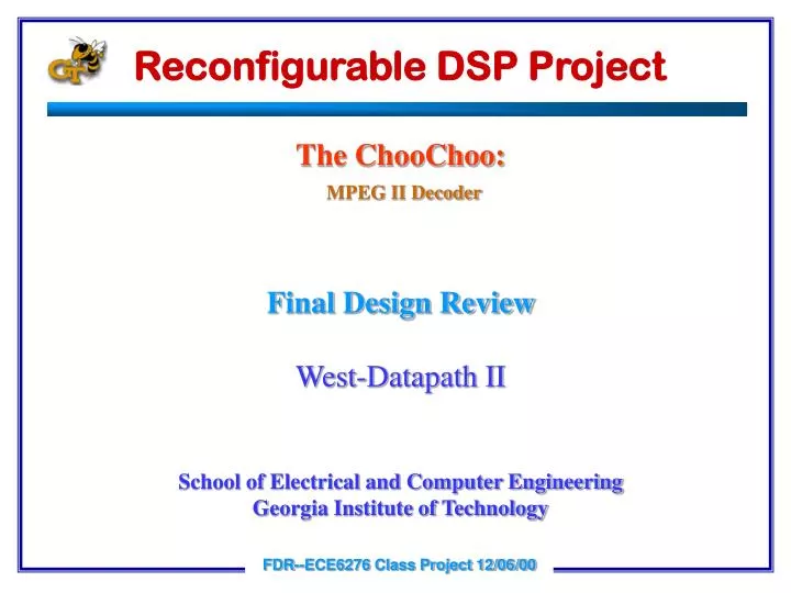
Reconfigurable DSP Project. The ChooChoo: Final Design Review West-Datapath II School of Electrical and Computer Engineering Georgia Institute of Technology. MPEG II Decoder. Team Members. Ravi Kondapalli Wesley Leong Joseph Long Asif Mahbub. Project Requirements.

E N D
Reconfigurable DSP Project The ChooChoo: Final Design Review West-Datapath II School of Electrical and Computer Engineering Georgia Institute of Technology MPEG II Decoder FDR--ECE6276 Class Project 12/06/00
Team Members • Ravi Kondapalli • Wesley Leong • Joseph Long • Asif Mahbub FDR--ECE6276 Class Project 12/06/00
Project Requirements • To design and test the switching mechanism for the three profiles • To compile, debug and test the DLX processor • To provide support role to other groups ( DP1, SIS) FDR--ECE6276 Class Project 12/06/00
Block Diagram Switch Controller Control Register DM 1 DM 2 Choo Choo DSP Profile 1 Profile 2 Profile 3 IM 3 IM 1 IM 2 FDR--ECE6276 Class Project 12/06/00
Profile Control Register • The global profile control register provides a switching mechanism between the three profiles of the signal processor. This register is located at the address 0xFFFFFFFF in the memory space of all three of the profiles. • Profile Control Register Bit allocation for the profiles: FDR--ECE6276 Class Project 12/06/00
Profile Data Memory Addressing • There is one single data memory that is shared between the three profiles. FDR--ECE6276 Class Project 12/06/00
P1_inst.mif DEPTH = 64; WIDTH = 32; ADDRESS_RADIX = HEX; DATA_RADIX = BIN; CONTENT BEGIN [0..3F] : 11111111111111111111111111111111 ; 00 : 01000000000000110000000000000001 ; -- ADDI R0, R3, #1 01 : 01001000000000110010000000000000 ; -- SUBR R0, R3, R4 02 : 01000000000000110000000000000010 ; -- ADDI R0, R3, #2 03 : 00100000100000000000000000001000 ; -- ST R4, R0, #8 04 : 00100000011001000000000000000000 ; -- ST R3, R4, #0 05 : 00100000011001000000000000000000 ; -- ST R3, R4, #0 END ; Profile 1 Test Program FDR--ECE6276 Class Project 12/06/00
P2_inst.mif DEPTH = 64; WIDTH = 32; ADDRESS_RADIX = HEX; DATA_RADIX = BIN; CONTENT BEGIN [0..3F] : 11111111111111111111111111111111 ; 00 : 00010000000000110000000000001000 ; -- LD R3, R0, #8 01 : 00000100000001000000000000000100 ; -- ADDI R4, R0, #4 02 : 00011000011001000000000000000000 ; -- ST R4, R3, #0 END ; Profile 2 Test Program FDR--ECE6276 Class Project 12/06/00
Switch Controller Simulation FDR--ECE6276 Class Project 12/06/00
Accomplishments • Control System Data Flow • UMA for Profile Memory • Debugged DLX code • Integration and Switching of Profiles • Global Control Register • One Bit per Profile • Writing to address 0xFFFFFFFF switches profiles • Test Switching of Profiles • Schedule was met FDR--ECE6276 Class Project 12/06/00
Conclusion • Difficulties Met: • DLX • Communicating with other groups • Support Roles: • DP1 • SIS FDR--ECE6276 Class Project 12/06/00