Download
1 / 30
340 likes | 621 Views
Counters. Dr. Rebhi S. Baraka rbaraka@iugaza.edu Logic Design (CSCI 2301) Department of Computer Science Faculty of Information Technology The Islamic University of Gaza. Outline. Asynchronous Counter Operation Synchronous Counter Operation Up/Down Synchronous Counters

E N D
Counters Dr. Rebhi S. Baraka rbaraka@iugaza.edu Logic Design (CSCI 2301) Department of Computer Science Faculty of Information Technology The Islamic University of Gaza
Outline • Asynchronous Counter Operation • Synchronous Counter Operation • Up/Down Synchronous Counters • Design of Synchronous Counters • Counter Application
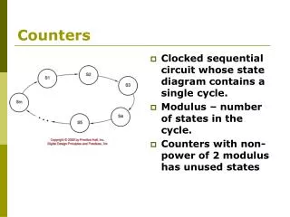
Asynchronous Counter Operation • A 2-Bit Asynchronous Binary Counter • FF0 is triggered by the clock; at the positive going edge of. • FF1 is triggered by the Q0 output of FF0; at the positive going transition.
A 3-Bit Asynchronous Binary Counter • FF0 is triggered by the clock; at the positive going edge of. • FF1 is triggered by the Q0 output of FF0; at the positive going transition. • FF2 is triggered by the Q1 output of FF1; at the positive going transition.
3-bit asynchronous binary counter and its timing diagram for one cycle.
A 4-Bit Asynchronous Binary Counter • FF0 is triggered by the clock; at the positive going edge of. • FF1 is triggered by the Q0 output of FF0; at the positive going transition. • FF2 is triggered by the Q1 output of FF1; at the positive going transition. • FF3 is triggered by the Q2 output of FF2; at the positive going transition.
Four-bit asynchronous binary counter and its timing diagram.
Asynchronous Decade Counters • These counters have 10 states in their sequence. • A decade counter of states from 0000 to 1001 is called a BCD decade counter. • Since the counter would have 16 states, it is forces to recycle before going through all of its possible state. • The BCD decade counter is recycled to 0000 after the 1001 state. • This is done as shown in the next slide by decoding count 1010 with an NAND gate and • connecting the output of the NAND gate to the clear inputs of the flip-flops. • What is Partial decoding? • Two unique states (in this case) are sufficient to decode the count of ten .
An asynchronously clocked decade counter with asynchronous recycling.
Synchronous Counter Operation • 2-Bit Synchronous Binary Counter • Both flip-flops are triggered by the clock. • FF0 is in the toggle mode. • The J and K inputs of FF1 are having 00 or 11 depending on Q0
Timing details for the 2-bit synchronous counter operation (the propagation delays of both flip-flops are assumed to be equal).
Synchronous BCD decade counter • J0 = K0 = 1 • J1 = K1 = Q0Q3 • J2 = K2 = Q0Q1 • J3 = K3 = Q0Q1Q2 + Q0Q3
Up/Down Synchronous Counters • Called also bidirectional counter • It is capable of progressing in either direction up or down in a certain sequence • We study 3-bit up/down synchronous counter
3-bit up/down synchronous counter J0 = K0 = 1 J1 = K1 = Q0·UP + Q0·DOWN J2 = K2 = Q0Q1·UP + Q0·Q1·DOWN
Design of Sequential Circuit • A sequential circuit (state machine) consists of a combinational logic section and a memory section (flip-flops).
Design of Sequential Circuit • The information in the memory and the inputs to them combinational logic are required for the operation of the circuit. • Not all sequential circuits are required to have inputs and outputs. • All sequential circuits have excitation variables and state variables.
Design Procedure for Sequential Circuits as Applied to Counters • Steps: • State diagram • Next-State Table • Transition Table • Karnaugh Maps • Input Logic • Implementation
State Diagram State diagram for a 3-bit Gray code counter.
Next-State Table Examples of the mapping procedure for the counter sequence represented.
Example: Designing a counter with the irregular binary sequence 1-> 2 -> 5 -> 7 We work this example entirely on the black board.
These slides are based on Digital Fundamentals 9th ed. By Thomas Floyd End of the slides