Download
1 / 20
200 likes | 418 Views
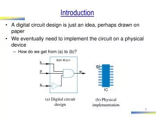
Introduction. A digital circuit design is just an idea, perhaps drawn on paper We eventually need to implement the circuit on a physical device How do we get from (a) to (b)?. B. elt. W. a. r. n. k. si. p. w. s. IC. (a) Digital circuit design. (b) Physical implementation. C. us.

E N D
Introduction • A digital circuit design is just an idea, perhaps drawn on paper • We eventually need to implement the circuit on a physical device • How do we get from (a) to (b)? B elt W a r n k si p w s IC (a) Digital circuit design (b) Physical implementation
C us t om l a y out F ab mo n ths IC Manufactured IC Technologies • We can manufacture our own IC • Months of time and millions of dollars • (1) Full-custom or (2) semicustom • (1) Full-custom IC • We make a fullcustom layout • Using CAD tools • Layout describes the location and size of every transistor and wire • A fab (fabrication plant) builds IC for layout • Hard! • Fab setup costs ("non-recurring engineering", or NRE, costs) high • Error prone (several "respins") • Fairly uncommon • Reserved for special ICs that demand the very best performance or the very smallest size/power B elt W a r n k p w s a
k p s ( d ) ( c ) IC F ab w eeks ( justwi r ing) Manufactured IC Technologies – Gate Array ASIC • (2) Semicustom IC • "Application-specific IC" (ASIC) • (a) Gate array or (b) standard cell • (2a) Gate array • Series of gates already layed out on chip • We just wire them together • Using CAD tools • Vs. full-custom • Cheaper and quicker to design • But worse performance, size, power • Very popular B elt W a r n k p w s ( b ) ( a ) w a
a'b ab' Manufactured IC Technologies – Gate Array ASIC • (2a) Gate array • Example: Mapping a half-adder to a gate array Half-adder equations: s = a'b + ab' co = ab a c o ab b s G a t e a r r a y a
d ( ) IC 1-3 months (cells and wiring) Manufactured IC Technologies – Standard Cell ASIC • (2) Semicustom IC • "Application-specific IC" (ASIC) • (a) Gate array or (b) standard cell • (2b) Standard cell • Pre-layed-out "cells" exist in library, not on chip • Designer instantiates cells into pre-defined rows, and connects • Vs. gate array • Better performance/power/size • A bit harder to design • Vs. full custom • Not as good of circuit, but still far easier to design BeltWarn k p w Cell library s b ( ) a ( ) w k p cell row s cell row cell row c ( ) Fab a
ab a'b a c o ab a'b ab' b ab' s Notice fewer gates and shorter wires for standard cells versus gate array, but at cost of more design effort G a t e a r r a y Manufactured IC Technologies – Standard Cell ASIC • (2b) Standard cell • Example: Mapping a half-adder to standard cells co = ab s = a'b + ab' co a s b cell row cell row cell row a a
Programmable IC Technology – FPGA • Manufactured IC technologies require weeks to months to fabricate • And have large (hundred thousand to million dollar) initial costs • Programmable ICs are pre-manufactured • Can implement circuit today • Just download bits into device • Slower/bigger/more-power than manufactured ICs • But get it today, and no fabrication costs • Popular programmable IC – FPGA • "Field-programmable gate array" • Developed late 1980s • Though no "gate array" inside • Named when gate arrays were very popular in the 1980s • Programmable in seconds
F = x'y' + xy 4x 2 Mem. G = xy' 4x 1 Mem. 1 rd x y F G 1 rd 1 0 10 0 1 0 0 1 0 0 1 00 1 0 0 1 0 0 0 2 01 2 0 1 0 0 1 x=0 1 3 10 3 1 a1 a1 x 1 1 1 0 a0 y a0 D1 D0 D y=0 F=1 F G c d e ( ) ( ) ( ) FPGA Internals: Lookup Tables (LUTs) • Basic idea: Memory can implement combinational logic • e.g., 2-address memory can implement 2-input logic • 1-bit wide memory – 1 function; 2-bits wide – 2 functions • Such memory in FPGA known as Lookup Table (LUT) F = x'y' + xy 4x 1 Mem. x y F 1 rd 0 0 1 0 0 1 0 1 1 0 0 2 1 1 1 3 a1 x a0 y D F a b ( ) ( ) a a a a
BeltWarn k p s w k 0 0 0 0 p w 0 0 1 0 0 1 0 0 0 1 1 0 s 1 0 0 0 a ( ) 1 0 1 0 1 1 0 1 8x 1 Mem. 1 1 1 0 0 0 b ( ) 1 0 2 0 Programming 3 0 (seconds) k a2 4 0 p a1 5 0 s a0 Fab 6 1 1-3 months 7 0 D C I c ( ) w FPGA Internals: Lookup Tables (LUTs) • Example: Seat-belt warning light (again) a a
Sub-circuits have only 3-inputs each kps' 8x 1 Mem. 8x 1 Mem. BeltWarn k 0 0 0 0 p x 1 0 1 1 w 2 0 2 1 s 3 0 3 1 x t k a2 a2 4 0 4 1 p a1 a1 d 5 0 5 1 s a0 a0 6 1 6 1 x+t+d 3 inputs 3 inputs 7 0 7 1 1 output 1 output D D x=kps' w=x+t+d t b ( ) d Partition circuit into 3-input sub-circuits w c ( ) FPGA Internals: Lookup Tables (LUTs) • Lookup tables become inefficient for more inputs • 3 inputs only 8 words • 8 inputs 256 words; 16 inputs 65,536 words! • FPGAs thus have numerous small (3, 4, 5, or even 6-input) LUTs • If circuit has more inputs, must partition circuit among LUTs • Example: Extended seat-belt warning light system: BeltWarn k p w s t d a ( ) 5-input circuit, but 3-input LUTs available Map to 3-input LUTs a a
FPGA Internals: Lookup Tables (LUTs) • Partitioning among smaller LUTs is more size efficient • Example: 9-input circuit a a 512x 1 M em. 3x1 b b c c d d e 3x1 e 3x1 F F f f 8x 1 M em. g g h h 3x1 i i ( b ) ( a ) ( c ) Partitioned among 3x1 LUTs Requires only 4 3-input LUTs (8x1 memories) – much smaller than a 9-input LUT (512x1 memory) Original 9-input circuit
0 0 0 0 0 0 1 0 0 0 0 0 0 0 1 0 0 0 0 0 0 0 1 0 0 0 1 0 0 1 1 0 t d F e Second column unused; first column implements AND/OR sub-circuit First column unused; second column implements AND FPGA Internals: Lookup Tables (LUTs) • LUT typically has 2 (or more) outputs, not just one • Example: Partitioning a circuit among 3-input 2-output lookup tables a 8x 2 Mem. 8x 2 Mem. b c 0 0 d 1 F 1 2 2 e a ( ) 3 3 a a2 a2 4 4 a a1 a1 1 b b 5 5 2 t c a0 a0 c 3 1 6 6 2 d 7 7 F 3 e D1 D0 D1 D0 b ( ) (Note: decomposed one 4-input AND input two smaller ANDs to enable partitioning into 3-input sub-circuits) a c ( ) a
10 00 01 00 Sub-circuit has 2 inputs, 2 outputs 00 10 00 01 0 0 00 00 i1 00 00 i0 00 00 00 00 Sub-circuit has 2 inputs, 2 outputs FPGA Internals: Lookup Tables (LUTs) • Example: Mapping a 2x4 decoder to 3-input 2-output LUTs d0 8x 2 Mem. 8x 2 Mem. 0 0 d1 1 1 2 2 d2 3 3 a2 a2 4 4 a1 a1 d3 5 5 a0 a0 6 6 7 7 D1 D0 D1 D0 i1 i0 a a d0 d1 d2 d3 a b ( ) ( )
Switch matrix 2-bit memory s1 s0 m0 i0 m1 o0 i1 4x 1 m2 d i2 mux m3 i3 o0 o1 m0 2-bit m1 memory m2 m3 Switch s1 s0 matrix i0 o1 i1 4x 1 d i2 mux i3 b ( ) FPGA Internals: Switch Matrices • Previous slides had hardwired connections between LUTs • Instead, want to program the connections too • Use switch matrices (also known as programmable interconnect) • Simple mux-based version – each output can be set to any of the four inputs just by programming its 2-bit configuration memory FPGA (partial) 8x 2 Mem. 8x 2 Mem. 0 00 0 00 1 00 1 00 2 00 2 00 P0 3 00 3 00 P6 P1 a2 a2 4 00 4 00 a1 a1 P2 P7 5 00 5 00 a0 a0 P3 6 00 6 00 7 00 7 00 D1 D0 D1 D0 P8 P9 P4 P5 a ( ) a a
Switch matrix s1 s0 m0 i0 m1 o0 i1 4x 1 m2 d i2 mux m3 i3 10 These bits establish the desired connections 11 s1 s0 i0 o1 i1 4x 1 d i2 mux i3 b ( ) FPGA Internals: Switch Matrices • Mapping a 2x4 decoder onto an FPGA with a switch matrix FPGA (partial) 8x 2 Mem. 8x 2 Mem. 10 0 10 0 00 1 01 1 00 2 00 2 10 0 3 00 3 01 d3 0 a2 a2 4 00 4 00 a1 a1 i1 d2 o0 5 00 5 00 a0 a0 i0 o1 m0 m1 6 00 6 00 11 m2 7 00 7 00 m3 Switch D1 D0 D1 D0 matrix d1 d0 i1 i0 a ( ) a
BeltWarn k p x w s t d FPGA Internals: Switch Matrices • Mapping the extended seatbelt warning light onto an FPGA with a switch matrix • Recall earlier example (let's ignore d input for simplicity) Switch matrix FPGA (partial) 8x 2 Mem. 8x 2 Mem. 00 0 0 0 0 0 0 1 0 0 1 0 1 s1 s0 m0 i0 2 0 0 2 0 1 m1 o0 0 i1 4x 1 3 0 0 3 0 1 m2 d w i2 mux k a2 a2 m3 4 0 0 4 00 i3 x a1 a1 p o0 00 5 0 0 5 00 a0 a0 s o1 m0 10 m1 6 0 1 6 00 10 m2 7 0 0 7 00 m3 Switch D1 D0 D1 D0 s1 s0 matrix i0 o1 i1 4x 1 d i2 mux t i3 0 a b ( ) ( ) a
CLB output flip-flop 1-bit 1 0 1 0 1 0 1 0 CLB 0 0 0 0 2x 1 2x 1 2x 1 2x 1 output configuration memory FPGA Internals: Configurable Logic Blocks (CLBs) • LUTs can only implement combinational logic • Need flip-flops to implement sequential logic • Add flip-flop to each LUT output • Configurable Logic Block (CLB) • LUT + flip-flops • Can program CLB outputs to come from flip-flops or from LUTs directly FPGA CLB CLB 8x 2 Mem. 8x 2 Mem. 0 00 0 00 1 00 1 00 2 00 2 00 P0 3 00 3 00 P1 a2 a2 4 00 4 00 a1 a1 P2 o0 00 5 00 5 00 a0 a0 P3 o1 m0 00 m1 6 00 6 00 m2 7 00 7 00 m3 Switch D1 D0 D1 D0 matrix P6 P7 P8 P9 P4 P5 a
11 00 10 01 01 10 00 11 0 00 00 a 10 00 00 b 11 00 00 00 00 1 1 1 1 z y x w c d FPGA Internals: Sequential Circuit Example using CLBs FPGA a b c d CLB CLB 8x 2 Mem. 8x 2 Mem. 0 0 1 1 2 2 0 3 3 a2 a2 4 4 w x y z a1 a1 o0 5 5 a ( ) a0 a0 o1 m0 m1 6 6 m2 7 7 m3 Left lookup table Switch D1 D0 D1 D0 matrix a2 a1 a0 D1 D0 0 a b w=a' x=b' 0 0 0 1 1 1 0 1 0 1 0 1 0 0 0 1 1 0 2 x1 2 x1 2 x1 2 x1 0 1 0 0 1 0 1 1 0 0 below unused b ( ) c ( ) a
FPGA Internals: Overall Architecture • Consists of hundreds or thousands of CLBs and switch matrices (SMs) arranged in regular pattern on a chip Connections for just one CLB shown, but all CLBs are obviously connected to channels Represents channel with tens of wires CLB CLB CLB SM SM CLB CLB CLB SM SM CLB CLB CLB
This isn't wrong. Although the bits appear as "10" above, note that the scan chain passes through those bits from right to left – so "01" is correct here. FPGA Internals: Programming an FPGA FPGA • All configuration memory bits are connected as one big shift register • Known as scan chain • Shift in "bit file" of desired circuit CLB CLB Pin 8x 2 Mem. 8x 2 Mem. 0 11 0 01 Pclk 1 10 1 00 2 01 2 11 0 3 01 3 10 0 a2 a2 4 00 4 00 a1 a a1 o0 10 5 00 5 00 a0 a0 b o1 m0 11 m1 6 00 6 00 a ( ) m2 7 00 7 00 m3 Switch D1 D0 D1 D0 matrix 2 x1 2x 1 2 x1 2 x1 1 1 1 1 z y x w c d b ( ) Pin Conceptual view of configuration bit scan chain is that of a 40-bit shift register Pclk a c ( ) Bit file contents for desired circuit: 1101011000000000111101010011010000000011


