Download
1 / 21
210 likes | 277 Views
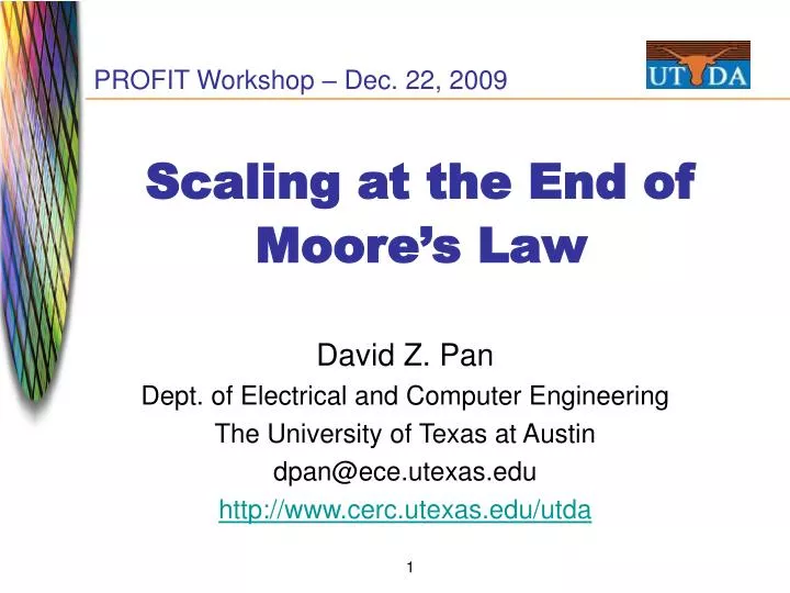
PROFIT Workshop – Dec. 22, 2009. Scaling at the End of Moore’s Law. David Z. Pan Dept. of Electrical and Computer Engineering The University of Texas at Austin dpan@ece.utexas.edu http://www.cerc.utexas.edu/utda. 10. [Courtesy Intel]. 1. um. 0.1. X. 2000. 2020. 1980. 1990. 2010.

E N D
PROFIT Workshop – Dec. 22, 2009 Scaling at the End of Moore’s Law David Z. Pan Dept. of Electrical and Computer Engineering The University of Texas at Austin dpan@ece.utexas.edu http://www.cerc.utexas.edu/utda
10 [Courtesy Intel] 1 um 0.1 X 2000 2020 1980 1990 2010 Moore’s Law & CMOS Scaling Lithography Gap! [Moore 1965]
-nce Scaling is Certainly Not Easy Litho CMP Etch Random defects
DFM to Rescue You Probably Have Seen This! • Scaling, though challenged, still pushing ahead! • Quite Amazing… Yes, we can! [Courtesy Synopsys]
Scaling at the End • Vertically – 3D IC • New devices/materials • E.g., Optical interconnect, high-K, strain silicon • Multi-core, many core, networks-on-chip • ……. • But still life in continuing pushing the envelope, 22nm, 16nm, 11nm, 8nm (ITRS) • Computational Scaling • Double Patterning • Emerging Nanolithography • … • E.g., Intel sees no problem for another decade
Computational Scaling • Scaling by massive computational power • Fast computers to help design faster computers • Computational lithography for nanolithography systems • Computationally reverse-engineering • Electronic design automation (EDA) eco-system to close the gaps • Current tools are still very sub-optimal • Synergistic Process-Layout-Circuit Co-Optimization • Parallel, multi-core, GPU, domain-specific, FPGA…
Computational Lithography Intel’s Pixelated Mask [Singh+, SPIE’08)
Design EDA Lever Synergistic CAD to the Rescue • CAD tools still very suboptimal • Need good levers at different levels of abstraction for process/layout/circuit co-opt. “Give me a place to stand on, and I can move the earth.” - Archimedes’ Lever “Give me a lever, and I can optimize your billion transistor design.” - EDA’s Lever (model/rule)
Litho model: Hopkins eqn CMP model: [Cho+, ICCAD’06] Process Modeling • How complicated? • or simple can it be? • Key Issues: • Accuracy vs. Fidelity (Elmore-like) • Design-oriented vs. process-oriented
Hotspot! Layout! Prediction & Prescription • Prediction: e.g., data mining, machine learning [Ding+, ICICDT’09] (Best Student Paper) • Prescription: only work with patterns that are printable • Robustness Design: tolerant to variations/aging, e.g. ,[Chakraborty+, DATE 2009] (Best IP Award)
193i w/ DPL mindp “Next” Generation Lithography EUV Nanoimprint
Double Patterning Lithography • For 22nm and 16nm, the industry most likely will adopt double patterning lithography (DPL) • A key problem is overlay control • Double exposures, masks, … • Intelligent CAD solution to compensate the unwanted overlay effects or even take advantage of them! • E.g., [Yang et al, ASPDAC’2010] (Best Paper Award Nomination) • A new layout decomposition framework
mindp Stitch A Faster & Versatile Framework • [Yang et al., ASPDAC 2010] proposed a new graph-theoretic, multi-objective layout decomposition framework • Consider new objectives • Density balancing • Overlay compensation • In addition to conventional metrics • Decomposability • Stitch minimization • Very efficient for full chip
Overlay Compensation 2nd patterning 2nd patterning C1 -∆C1 C2 -∆C2 1st patterning 1st patterning Decomposition Without Overlay Compensation 2nd patterning 1st patterning C2 +∆C2 C1 -∆C1 2nd patterning 1st patterning Decomposition With Overlay Compensation (for Timing Variation Reduction)
Color Assignment – Heuristic Solution The number of stitches in layout decomposition is equal to the cut size of the bi-partitioning problem in graph theory. Theorem 1 : Min-Cut Based Stitch Minimization E A Example of Graph Based Stitch Minimization Ā(20) Ē Ā 2 1 A(17) X(9) E A Ē Ā 1 Z(5) X Y Z Ē(17) 1 E(15) E A 2 Ē Ā Y(9) 1 Constraint: (A, Ā) and (E, Ē) are repulsive pairs. Minimize : A⊕X + X⊕Z + Y⊕Z + E⊕Y + 2(Ā⊕X) + 2(Ē⊕Y)
Balancing Density is Easy Min-Stitch Coloring Balanced Coloring Ā(20) Ā(20) 2 1 A(17) A(17) 1 X(9) 2 X(9) 1 Z(5) 1 Z(5) 1 Ē(17) Ē(17) 1 E(15) E(15) Y(9) 2 2 1 Y(9) 1 Color1 Area =46 (50%) Color0 Area =46 (50%) Color0 Area =32 (35%) Color1 Area=60 (65%) E A E A Ē Ā Ē Ā E A E A Ē Ā Ē Ā X Y Z X Y Z E A E A Ē Ā Ē Ā 16
Compensate Overlay Effect color0 color1 x1 x1’ Cc2 Cc1 Cc2 Cc1 1 i1 1 x2 x2’ R1 R2 R3 Rd 1 R4 R1 R2 R3 Rd R4 i2 1 y1’ y1 R5 R5 1 i3 Cc3 Cc3 y2 y2’ TDD 1 # of Stitch=2 R6 R6 without TDD constraints R7 R7 Cc4 Cc4 x1 x1’ 1 w i1 1 x1’ x2’ x2 x2’ 1 i2 1 x1 i1 x2 i2 y1’ y1 w 1 i3 y2 y2’ y1’ y1 1 i3 y2 y2’ TDD constraints insertion Relative coloring
Experimental Results • [Yang et al., ASPDAC 2010] very fast (cf. ILP) • It handles density balancing nicely 18
How about post-16nm? • Triple patterning • Quadruple patterning • Intel 7nm • Extreme Ultra-Violet Lithography (13.5nm) • Massively e-beam direct write • Nanoimprint [Intel, July 2009]
Still 50 Years Ago, … There's Plenty of Room at the Bottom - An Invitation to Enter a New Field of Physics Richard P. Feynman, 1959 The Moore, The Better!