Download
1 / 1

E N D
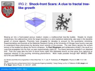
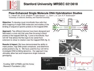
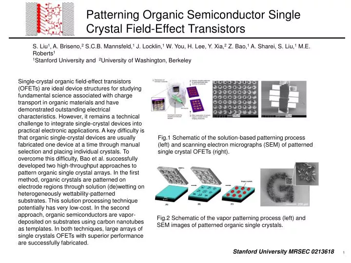
Single-crystal organic field-effect transistors (OFETs) are ideal device structures for studying fundamental science associated with charge transport in organic materials and have demonstrated outstanding electrical characteristics. However, it remains a technical challenge to integrate single-crystal devices into practical electronic applications. A key difficulty is that organic single-crystal devices are usually fabricated one device at a time through manual selection and placing individual crystals. To overcome this difficulty, Bao et al. successfully developed two high-throughput approaches to pattern organic single crystal arrays. In the first method, organic crystals are patterned on electrode regions through solution (de)wetting on heterogeneously wettability-patterned substrates. This solution processing technique potentially has very low-cost. In the second approach, organic semiconductors are vapor-deposited on substrates using carbon nanotubes as templates. In both techniques, large arrays of single crystals OFETs with superior performance are successfully fabricated. Patterning Organic Semiconductor Single Crystal Field-Effect Transistors S. Liu1, A. Briseno,2 S.C.B. Mannsfeld,1 J. Locklin,1 W. You, H. Lee, Y. Xia,2 Z. Bao,1 A. Sharei, S. Liu,1 M.E. Roberts1 1Stanford University and 2University of Washington, Berkeley Fig.1 Schematic of the solution-based patterning process (left) and scanning electron micrographs (SEM) of patterned single crystal OFETs (right). a Fig.2 Schematic of the vapor patterning process (left) and SEM images of patterned organic single crystals. 10 μm Stanford University MRSEC 0213618 1